Main Content

Buck Converter

Controller-driven DC-DC step-down voltage regulator

  • Buck Converter block

Libraries:
Simscape / Electrical / Semiconductors & Converters / Converters

Description

The Buck Converter block represents a converter that steps down DC voltage as driven by an attached controller and gate-signal generator. Buck converters are also known as step-down voltage regulators because they decrease voltage magnitude.

The Buck Converter block allows you to model a nonsynchronous converter with one switching device or a synchronous converter with two switching devices. Options for the type of switching devices are:

  • GTO — Gate turn-off thyristor. For information about the I-V characteristic of the device, see GTO.

  • Ideal semiconductor switch — For information about the I-V characteristic of the device, see Ideal Semiconductor Switch.

  • IGBT — Insulated-gate bipolar transistor. For information about the I-V characteristic of the device, see IGBT (Ideal, Switching).

  • MOSFET — N-channel metal-oxide-semiconductor field-effect transistor. For information about the I-V characteristic of the device, see MOSFET (Ideal, Switching).

  • Thyristor — For information about the I-V characteristic of the device, see Thyristor (Piecewise Linear).

  • Averaged Switch — Semiconductor switch with an antiparallel diode. The control signal port G accepts values in the interval [0,1]. When G is equal to 0 or 1, the averaged switch is fully opened or fully closed respectively. The switch behaves similarly to the Ideal Semiconductor Switch block with an antiparallel diode. When G is between 0 and 1, the averaged switch is partly opened. You can average the pulse-width modulation (PWM) signal over a specified period. You can then undersample the model and use modulation waveforms instead of PWM signals.

Converter Topology

You can model this converter as a nonsynchronous converter with a physical signal gate control port or with two electrical control ports, or as a synchronous converter with an electrical control port. To select the converter topology, set the Modeling option parameter to either:

  • Nonsynchronous converter — Nonsynchronous converter with optional physical or electrical gate control ports.

  • Synchronous converter — Synchronous converter with multiplexed gate signals.

The nonsynchronous buck converter models contain a switching device, a diode, an inductor, and an output capacitor.

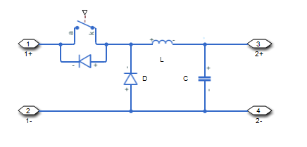
The synchronous buck converter model contains two switching devices, an inductor, and an output capacitor.

In each case, the capacitor smoothes the output voltage.

Protection

For the synchronous converter model, you can include an integral protection diode for the S2 switching device. An integral diode protects the semiconductor device by providing a conduction path for reverse current. An inductive load can produce a high reverse-voltage spike when the semiconductor device suddenly switches off the voltage supply to the load.

To include and configure the internal protection diode block, use the Diode parameters. This table shows how to set the Model dynamics parameter based on your goals.

GoalsValue to SelectIntegral Protection Diode
Do not include protection.NoneNone
Include protection.Prioritize simulation speed.Diode with no dynamicsThe Diode block
Prioritize model fidelity by precisely specifying reverse-mode charge dynamics.Diode with charge dynamicsThe dynamic model of the Diode block

You can also include a snubber circuit for each switching device. Snubber circuits contain a series-connected resistor and capacitor. They protect switching devices against high voltages that inductive loads produce when the device turns off the voltage supply to the load. Snubber circuits also prevent excessive rates of current change when a switching device turns on.

To include and configure a snubber circuit for each switching device, use the Snubbers parameters.

Gate Control

To connect gate-control voltage signals to the gate ports of the switching devices, for the:

  • Nonsynchronous converter model:

    • PS control port model:

      1. Convert a Simulink® gate-control voltage signal to a physical signal using a Simulink-PS Converter block.

      2. Connect the Simulink-PS Converter block to the G port.

    • Electrical control ports model:

      1. Connect a Simscape™ electrical-domain positive DC voltage signal to the G+ port.

      2. Connect the Simscape electrical-domain negative DC voltage signal to the G- port.

  • Synchronous converter model:

    1. Convert each Simulink gate-control voltage signal to a physical signal using Simulink-PS Converter blocks.

    2. Multiplex the converted gate-control signals into a single vector using a Two-Pulse Gate Multiplexer.

    3. Connect the vector signal to the G port.

Piecewise Constant Approximation in Averaged Switch for FPGA Deployment

If you set the Switching device parameter to Averaged switch and your model uses a partitioning solver, this block produces nonlinear partitions because the average mode equations include modes, Gsat that are functions of the input G. To make these equations compatible with hardware description language (HDL) code generation, and therefore FPGA deployment, set the Integer for piecewise constant approximation of gate input (0 for disabled) parameter to a value greater than 0. This block then treats the Gsat mode as a piecewise constant integer with a fixed range. This turns the previously nonlinear partitions to linear time varying partitions.

An integer value in the range [0,K], where K is the value of the Integer for piecewise constant approximation of gate input (0 for disabled), is now associated with each real value mode in the range [0,1]. The block computes the piecewise constant mode by dividing the original mode by K to normalize it back to the range [0,1]:

uI=(floor(uK))u^=uIK

Variables

To set the priority and initial target values for the block variables before simulation, use the Initial Targets section in the block dialog box or Property Inspector. For more information, see Set Priority and Initial Target for Block Variables.

Nominal values provide a way to specify the expected magnitude of a variable in a model. Using system scaling based on nominal values increases the simulation robustness. You can specify nominal values using different sources, including the Nominal Values section in the block dialog box or Property Inspector. For more information, see System Scaling by Nominal Values.

Assumptions and Limitations

Only a PWM-driven averaged switch converter captures both continuous conduction mode (CCM) and discontinuous conduction mode (DCM). A duty cycle-driven averaged switch converter captures CCM only.

Ports

Input

expand all

Physical signal port associated with the gate terminals of the switching device.

Dependencies

To enable this port, set Modeling option to Nonsynchronous converter and Gate-control port to PS.

Data Types: double

Conserving

expand all

Electrical conserving port associated with the gate terminals of the switching devices.

Dependencies

To enable this port, set Modeling option to Synchronous converter.

Data Types: double

Positive electrical conserving port associated with the positive gate terminal of the switching device.

Dependencies

To enable this port, set Modeling option to Nonsynchronous converter and Gate-control port to Electrical.

Data Types: double

Negative electrical conserving port associated with the negative gate terminal of the switching device.

Dependencies

To enable this port, set Modeling option to Nonsynchronous converter and Gate-control port to Electrical.

Data Types: double

Electrical conserving port associated with the positive terminal of the first DC voltage.

Data Types: double

Electrical conserving port associated with the negative terminal of the first DC voltage.

Data Types: double

Electrical conserving port associated with the positive terminal of the second DC voltage.

Data Types: double

Electrical conserving port associated with the negative terminal of the second DC voltage.

Data Types: double

Parameters

expand all

Whether to model nonsynchronous or synchronous converter.

Switching Devices

This table shows how the visibility of Switching Devices parameters depends on the Switching device that you select. To learn how to read the table, see Parameter Dependencies.

Switching Devices Parameter Dependencies

Parameters and Options
Switching device
Ideal Semiconductor SwitchGTOIGBTMOSFETThyristorAveraged Switch
On-state resistanceForward voltageForward voltageDrain-source on resistanceForward voltageOn-state resistance
Off-state conductanceOn-state resistanceOn-state resistanceOff-state conductanceOn-state resistance
Threshold voltageOff-state conductanceOff-state conductanceThreshold voltageOff-state conductance
Gate trigger voltage, VgtThreshold voltageGate trigger voltage, VgtInteger for piecewise constant approximation of gate input (0 for disabled)
Gate turn-off voltage, Vgt_offGate turn-off voltage, Vgt_off
Holding currentHolding current

Whether to specify physical or electrical control port for the switching gate.

Dependencies

To enable this port, set Modeling option to Nonsynchronous converter.

Switching device type for the converter. For the synchronous model, the switches are identical.

Dependencies

See the Switching Devices Parameter Dependencies table.

For the different switching device types, the Forward voltage is taken as:

  • GTO — Minimum voltage required across the anode and cathode block ports for the gradient of the device I-V characteristic to be 1/Ron, where Ron is the value of On-state resistance

  • IGBT — Minimum voltage required across the collector and emitter block ports for the gradient of the diode I-V characteristic to be 1/Ron, where Ron is the value of On-state resistance

  • Thyristor — Minimum voltage required for the device to turn on

Dependencies

See the Switching Devices Parameter Dependencies table.

For the different switching device types, the On-state resistance is taken as:

  • GTO — Rate of change of voltage versus current above the forward voltage

  • Ideal semiconductor switch — Anode-cathode resistance when the device is on

  • IGBT — Collector-emitter resistance when the device is on

  • Thyristor — Anode-cathode resistance when the device is on

  • Averaged Switch — Anode-cathode resistance when the device is on

Dependencies

See the Switching Devices Parameter Dependencies table.

Resistance between the drain and the source, which also depends on the gate-to-source voltage.

Dependencies

See the Switching Devices Parameter Dependencies table.

Conductance when the device is off. The value must be less than 1/R, where R is the value of On-state resistance.

For the different switching device types, the On-state resistance is taken as:

  • GTO — Anode-cathode conductance

  • Ideal semiconductor switch — Anode-cathode conductance

  • IGBT — Collector-emitter conductance

  • MOSFET — Drain-source conductance

  • Thyristor — Anode-cathode conductance

Dependencies

See the Switching Devices Parameter Dependencies table.

Gate voltage threshold. The device turns on when the gate voltage is above this value. For the different switching device types, the device voltage of interest is:

  • Ideal semiconductor switch — Gate-cathode voltage

  • IGBT — Gate-emitter voltage

  • MOSFET — Gate-source voltage

Dependencies

See the Switching Devices Parameter Dependencies table.

Gate-cathode voltage threshold. The device turns on when the gate-cathode voltage is above this value.

Dependencies

See the Switching Devices Parameter Dependencies table.

Gate-cathode voltage threshold. The device turns off when the gate-cathode voltage is below this value.

Dependencies

See the Switching Devices Parameter Dependencies table.

Gate current threshold. The device stays on when the current is above this value, even when the gate-cathode voltage falls below the gate trigger voltage.

Dependencies

See the Switching Devices Parameter Dependencies table.

Integer used to perform piecewise constant approximation of the gate input for FPGA deployment.

Dependencies

To enable this parameter, set Switching device to Averaged Switch.

Diode

This table shows how the visibility of Diode parameters depends on how you configure the Modeling option, Model dynamics, and Reverse recovery time parameterization parameters. To learn how to read this table, see Parameter Dependencies.

Diode Parameter Dependencies

Parameters and Options
Modeling option
PS control port or Electrical control portsSynchronous converter
Model dynamicsModel dynamics
Diode with no dynamicsDiode with charge dynamicsNoneDiode with no dynamicsDiode with charge dynamics
Forward voltageForward voltageForward voltageForward voltage
On resistanceOn resistanceOn resistanceOn resistance
Off conductanceOff conductanceOff conductanceOff conductance
Junction capacitanceJunction capacitance
Peak reverse current, iRMPeak reverse current, iRM
Initial forward current when measuring iRMInitial forward current when measuring iRM
Rate of change of current when measuring iRMRate of change of current when measuring iRM
Reverse recovery time parameterizationReverse recovery time parameterization
Specify stretch factorSpecify reverse recovery time directlySpecify reverse recovery chargeSpecify stretch factorSpecify reverse recovery time directlySpecify reverse recovery charge
Reverse recovery time stretch factorReverse recovery time, trrReverse recovery charge, QrrReverse recovery time stretch factorReverse recovery time, trrReverse recovery charge, Qrr

Diode type. The options are:

  • None — This option is not available for the nonsynchronous converter.

  • Diode with no dynamics — Select this option to prioritize simulation speed using the Diode block. This option is the default for the nonsynchronous converter.

  • Diode with charge dynamics — Select this option to prioritize model fidelity in terms of reverse mode charge dynamics using the commutation diode model of the Diode block.

Note

If you select Averaged Switch for the Switching Device parameter in the Switching Device setting, this parameter is not visible and Diode with no dynamics is automatically selected.

Dependencies

See the Diode Parameter Dependencies table.

Minimum voltage required across the positive and negative block ports for the gradient of the diode I-V characteristic to be 1/Ron, where Ron is the value of On resistance.

Rate of change of voltage versus current above the Forward voltage.

Conductance of the reverse-biased diode.

Diode junction capacitance.

Dependencies

See the Diode Parameter Dependencies table.

Peak reverse current measured by an external test circuit.

Dependencies

See the Diode Parameter Dependencies table.

Initial forward current when measuring peak reverse current. This value must be greater than zero.

Dependencies

See the Diode Parameter Dependencies table.

Rate of change of current when measuring peak reverse current.

Dependencies

See the Diode Parameter Dependencies table.

Model for parameterizing the recovery time. When you select Specify stretch factor or Specify reverse recovery charge, you can specify a value that the block uses to derive the reverse recovery time.

Dependencies

See the Diode Parameter Dependencies table.

Value that the block uses to calculate Reverse recovery time, trr. Specifying the stretch factor is an easier way to parameterize the reverse recovery time than specifying the reverse recovery charge. The larger the value of the stretch factor, the longer it takes for the reverse recovery current to dissipate.

Dependencies

See the Diode Parameter Dependencies table.

Interval between the time when the current initially goes to zero (when the diode turns off) and the time when the current falls to less than 10 percent of the peak reverse current.

The value of the Reverse recovery time, trr parameter must be greater than the value of the Peak reverse current, iRM parameter divided by the value of the Rate of change of current when measuring iRM parameter.

Dependencies

See the Diode Parameter Dependencies table.

Value that the block uses to calculate Reverse recovery time, trr. Use this parameter if the data sheet for your diode device specifies a value for the reverse recovery charge instead of a value for the reverse recovery time.

The reverse recovery charge is the total charge that continues to dissipate when the diode turns off. The value must be less than i2RM2a,

where:

  • iRM is the value specified for Peak reverse current, iRM.

  • a is the value specified for Rate of change of current when measuring iRM.

Dependencies

See the Diode Parameter Dependencies table.

LC Filter

Inductance of the LC filter.

Series resistance of the inductor.

Capacitance of the LC filter.

Series resistance of the capacitor.

Snubbers

The Snubbers parameters tab is not visible if you set Switching device to Averaged Switch.

The table summarizes the Snubbers parameter dependencies. To learn how to read the table, see Parameter Dependencies.

Snubbers Parameter Dependencies

Snubbers Parameter Dependencies
Snubber
NoneRC Snubber
Snubber resistance
Snubber capacitance

Switching device snubber.

Dependencies

See the Snubbers Parameter Dependencies table.

Resistance of the switching device snubber.

Dependencies

See the Snubbers Parameter Dependencies table.

Capacitance of the switching device snubber.

Dependencies

See the Snubbers Parameter Dependencies table.

References

[1] Trzynadlowski, A. M. Introduction to Modern Power Electronics, 2nd Edition. Hoboken, NJ: John Wiley & Sons Inc., 2010.

[2] Hedayati, M. H., P. Bharadwaj, and V. John. "Hybrid synchronous DC-DC buck power converter using Si and GaN transistors." IEEE International Conference on Power Electronics, Drives and Energy Systems (PEDES). Trivandrum, India: 2016, pp 1-6.

Extended Capabilities

C/C++ Code Generation
Generate C and C++ code using Simulink® Coder™.

Version History

Introduced in R2018a