Deploy and Verify HDL Neural Network Based DPD on FPGA
This example shows how to deploy a neural-network-based digital predistorter (NN DPD) algorithm on the Xilinx® Zynq® UltraScale+(TM) MPSoC ZCU102 board and verify the deployed NN DPD algorithm using an orthogonal frequency-division multiplexing (OFDM) signal.
The NN DPD application consists of two main modules: a preprocessing module and a neural network module. The preprocessing module calculates the amplitudes of the Iin/Qin samples up to the kth power. This calculation is crucial to account for the nonlinearity of the power amplifier (PA). The resulting amplitudes are used as inputs for the subsequent neural network module. The neural network module consists of multiple fully connected layers and ReLU layers. These layers perform feature extraction and detection for effective predistortion of the input signals. For more information about NN DPD, see Neural Network for Digital Predistortion Design-Offline Training (Communications Toolbox).
To begin the deployment process, ensure that the SD card of the board is set up properly. For more information, see Guided SD Card Setup (Deep Learning HDL Toolbox).
To run this example, perform these steps:
Configure the deep learning processor and generate IP core.
Model the design under test (DUT), including preprocessing modules for calculating the amplitudes and handshaking logic with the deep learning processor.
Generate and deploy the bitstream on the FPGA.
Compile and deploy the NN DPD on the FPGA.
Verify the deployed DPD using MATLAB®.
Configure Deep Learning Processor and Generate IP Core
The deep learning processor IP core accesses the preprocessed input from the DDR memory, performs the distortion, and loads the output back into the memory. To generate the deep learning processor IP core with the required interfaces, create a deep learning processor configuration by using the dlhdl.ProcessorConfig (Deep Learning HDL Toolbox)InputRunTimeControl and OutputRunTimeControl parameters to register mode. These parameters indicate the interface type between the input and output of the deep learning processor. To learn about these parameters, see Interface with the Deep Learning Processor IP Core (Deep Learning HDL Toolbox).
 hPC = dlhdl.ProcessorConfig;
 hPC.InputRunTimeControl = "register";
 hPC.OutputRunTimeControl = "register";
Specify the TargetPlatform property of the processor configuration object as Generic Deep Learning Processor. This option generates a custom generic deep learning processor IP core.
hPC.TargetPlatform = 'Generic Deep Learning Processor';
Use the setModuleProperty method to set the properties of the conv module of the deep learning processor. You can tune these parameters based on the design choice to ensure that the design fits on the FPGA. To learn more about these parameters, see setModuleProperty (Deep Learning HDL Toolbox)ModuleGeneration is turned off for convolutional layers and custom layers. InputMemorySize and OutputMemorySize are set to 1024.
 hPC.setModuleProperty('conv','ModuleGeneration', 'off');
 hPC.setModuleProperty('custom','ModuleGeneration', 'off');
 hPC.setModuleProperty('fc','FCThreadNumber',16);
 hPC.setModuleProperty('fc','InputMemorySize',1024);
 hPC.setModuleProperty('fc','OutputMemorySize',1024);
Use the hdlsetuptoolpath function to add the Xilinx Vivado synthesis tool path to the system path.
hdlsetuptoolpath('ToolName','Xilinx Vivado','ToolPath','C:\Xilinx\Vivado\2023.1\bin\vivado.bat');Use the dlhdl.buildProcessor function with the hPC object to generate the deep learning IP core. It takes some time to generate the deep learning processor IP core.
dlhdl.buildProcessor(hPC);
The generated IP core contains a standard set of registers and the generated IP core report. The IP core report is generated in the same folder as an IP core with the name testbench_ip_core_report.html.

You require IP core name and IP core folder in the subsequent step Set Target Reference Design task of the DUT IP core generation workflow. The IP core report contains the address map of the registers that are needed for handshaking with the input and output of deep learning processor IP core.
The registers InputValid, InputAddr, and InputSize contain the values of the corresponding handshaking signals that are required to write the preprocessed frame into DDR memory. After the data is written into memory, the DUT uses the register InputNext to pulse the inputNext signal. These register addresses are set up in the zynqHWSWHDLNNDPDInputGeneration script. For more details on interface signals, see the Design Processing Mode Interface Signals section of Interface with the Deep Learning Processor IP Core (Deep Learning HDL Toolbox).
Model Design Under Test
The model contains a preprocessing algorithm and handshaking algorithm. For more information, see HDL Neural Network Design for Digital Predistorter (Wireless HDL Toolbox).
modelName = 'zynqRadioHWSWDPDPreprocessTestbench';
open_system(modelName);

% Run the input generation script to create inputs to the model.
zynqRadioHWSWNNDPDInputGeneration;

Run the input generation script zynqRadioHWSWNNDPDInputGeneration each time you update the input generation parameters.
The reference design contains an ADI AXI DMA Controller to move the data from the processor to the FPGA fabric. The data is sent from the ARM processing system, through the DMA controller and AXI4-Stream interface, to the generated DUT Preprocessing IP core. The DUT contains two AXI Master interfaces. One AXI interface is connected to the Deep Learning Processor IP core and the other is connected to the DDR memory interface generator (MIG) IP.

Start the targeting workflow by right-clicking the DPD Preprocess DUT subsystem and selecting HDL Code > HDL Workflow Advisor.
In step 1.1, select
IP Core Generationworkflow and the platformXilinx Zynq Ultrascale+ MPSoC ZCU102 Evaluation Kit.

In step 1.2, set the reference design to
Deep Learning with Preprocessing Interface for Wireless Applications. The DL Processor IP name and location are obtained from the IP core report. These fields need to be filled appropriately. DL Processor IP vendor should be updated to 'mathworks.com'.

In step 1.3, map the target platform interfaces to the input and output ports of the DUT.
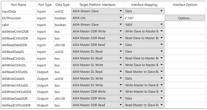
AXI4-Stream Slave Interface — The inputData and valid ports of the DUT are mapped to the Data and Valid ports of the AXI4-Stream Slave interface, respectively.
AXI4-Lite Interface — The DUTProcstart register is mapped to the AXI4-Lite register. When this register is written, it triggers the input handshaking process. Choosing the AXI4-Lite interface directs HDL Coder to generate a memory-mapped register in the FPGA fabric. You can access this register from software by running on the ARM processor. Other ports such as readInputStart, inputOffAddr and burstLen are also mapped to AXI4-Lite.
AXI4 Master DDR Interface — The AXIWriteCtrlInDDR, AXIReadCtrlInDDR, AXIReadDataDDR, AXIWriteCtrlOutDDR, AXIWriteDataDDR, and AXIReadCtrlOutDDR ports of the DUT are mapped to the AXI4 Master DDR interface. The read channel of the AXI4 Master DDR interface is mapped to the AXI4 Master DDR Read interface, and the write channel of the AXI4 Master DDR interface is mapped to the AXI4 Master DDR Write interface. This interface is used for the data transfer between the Preprocess DUT and the PL DDR. Using the Write Channel of this interface, the preprocessed data is written to the PL DDR which can then be accessed by the Deep Learning Processor IP.
AXI4 Master DL Interface — The AXIReadDataDL, AXIReadCtrlInDL, AXIWriteCtrlInDL, AXIReadCtrlOutDL, AXIWriteDataDL, and AXIWriteCtrlOutDL ports of the DUT are mapped to the AXI4 Master DL interface. The read channel of the AXI4 Master DL interface is mapped to the AXI4 Master DL Read interface, and the write channel of the AXI4 Master DL interface is mapped to the AXI4 Master DL Write interface. This interface is used for the communication between Preprocess DUT and the Deep Learning Processor IP. In this example, this interface is used for implementing input handshaking logic with Deep Learning Processor IP.
Step 2 prepares the design for HDL code generation.
Step 3 generates HDL code for the IP core.
Step 4.1 integrates the newly generated IP core into the reference design.
In step 4.2, the host interface script and Zynq software interface model is created. Since this example uses the interface script, and not the model, clear Generate Simulink software interface model. The host interface script,
gs_zynqHWSWNNDPDPreprocessTestbench_interface, which is generated in this step is parameterized and provided as thesetupPreprocessIPInterfacesfunction as part of this example.

Step 4.3 generates the bitstream. The bit file is named
block_design_wrapper.bitand located athdl_prj\vivado_ip_prj\vivado_prj.runs\impl_1. Copy the file to the present working folderpwd.
Compile and Deploy DPD Deep Learning Network
After generating the bitstream for the DUT integrated with the reference design that contains the DL IP core, deploy the end-to-end deep learning application onto an FPGA.
Create a target object to connect your target device to the host computer. Use the installed Xilinx Vivado Design Suite over an Ethernet connection to program the device.
hTarget = dlhdl.Target('Xilinx','Interface','Ethernet','IpAddr','192.168.1.101');Load the pretrained DPD object detection network.
load('savedNetNIVST100MHzHDL.mat');
net = netDPD;
Update the bitstream build information in the MAT file, generated during the IP core generation. The name of the MAT file is dlprocessor and is located in pwd\dlhdl_prj\, where pwd is your present working folder. Copy the file to the present working folder. This MAT file generated using the target platform Generic Deep Learning Processor does not contain the board and vendor information. To update the board and vendor information, use the updateBitStreamBuildInfo function and generate a new MAT file with the same name as generated bitstream.
   bitstreamName = 'block_design_wrapper';
   updateBitStreamBuildInfo('dlprocessor.mat',[bitstreamName,'.mat']);
Create a deep learning HDL workflow object using the dlhdl.Workflow class.
hW = dlhdl.Workflow('Network',net,'Bitstream',[bitstreamName,'.bit'],'Target',hTarget);Compile the network, net using the dlhdl.Workflow object.
   frameBufferCount = 5000;
   compile(hW, 'InputFrameNumberLimit', frameBufferCount);
Create a Xilinx processor hardware object and connect to the processor on-board the Xilinx SoC board.
hSOC = xilinxsoc('192.168.1.101', 'root', 'root');Call the xilinxsoc object function ProgramFPGA to program the FPGA and set the device tree to use the processor on the SoC board.
programFPGA(hSOC, [bitstreamName,'.bit'], 'devicetree_vision_dlhdl.dtb');
Run the deploy function of the dlhdl.Workflow object to download the network weights and biases on the Zynq UltraScale+ MPSoC ZCU102 board.
deploy(hW, 'ProgramBitStream', false);
Clear the DLHDL workflow object and hardware target.
   clear hW;
   clear hTarget;
Verify Deployed Digital Predistorter Using MATLAB
To verify the deployed DPD network using MATLAB, use the DPDDeployAndVerification function. This function contains the following scripts:
zynqHWSWNNDPDInputGeneration— Generate an OFDM signal for the input to the NN DPD. To generate the OFDM signal, set the bandwidth and modulation scheme in the InputGeneration block in the Simulink model. The bandwidth options are 100 MHz, 40 MHz, 15 MHz, and 5 MHz. The modulation scheme options are 64-QAM, 16-QAM, QPSK, and BPSK. ThetrainNowoption is available for training the neural network.
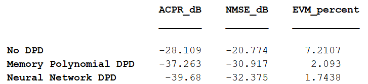
zynqHWSWNNDPDOutputVerification— Verify the collected output from NN DPD using PA. You can choose NI-VST PA or the simulated PA in InputGeneration block in the Simulink model. This script compares the NN DPD outptut with acomm.DPD(Communications Toolbox) object and calculates the power spectral density (PSD), adjacent channel power ration (ACPR), normalized mean squared error (NMSE), and error vector magnitude (EVM) values.
DPDDeployAndVerification(hSOC,modelName);
The DPDDeployAndVerification function uses the hSOC object as input and performs the following steps:
Generate the OFDM signal using the
zynqHWSWNNDPDInputGenerationscript as an input to the NN DPD for the verification process.Divide the OFDM signal into multiple bursts, where the NN DPD processes each burst at a time. In this example, the OFDM signal is divided into 28 bursts per OFDM symbol.
Upsample each burst of data by 36 times and pack it into a 32-bit data format. The real part is placed in 15 bits of MSB, the imaginary part is placed in the next 15 bits and the valid signal on 1 bit. The extra 1 bit on the LSB is left idle.
Upsample the data additionally by 4 to convert the 32-bit data to 128-bit data, as the preprocess algorithm reads 128-bit data from DDR memory.
Writes the burst of data into DDR memory using the address location on the port
inputOffAddr.After writing the data into DDR memory, assert all the necessary input signals:
inputStart,DUTProcStart,burstLen,readInputStart, andinputOffAddr.Check for the
outputValidsignal to ensure the availability of valid output after asserting all the inputs.Collect the NN DPD output data only when the
outputValidsignal is high.Assert
inputStopsignal high to stop the NN DPD from processing the input and setDUTProcStartto low.Verify the collected output using the
zynqHWSWNNDPDOutputVerificationscript.
The following figure shows the PSD plot for a bandwidth of 100 MHz and a modulation scheme of 16-QAM. The NMSE, ACPR, and EVM results are also shown to understand the performance of NN DPD compared to comm.DPD object and no-DPD scenarios.

See Also
comm.DPD (Communications Toolbox) | setModuleProperty (Deep Learning HDL Toolbox) | dlhdl.ProcessorConfig (Deep Learning HDL Toolbox)
Topics
- HDL Neural Network Design for Digital Predistorter (Wireless HDL Toolbox)
- Neural Network for Digital Predistortion Design - Online Training (Communications Toolbox)
- Deploy and Verify YOLO v2 Vehicle Detector on FPGA (Vision HDL Toolbox)
- Power Amplifier Characterization (Communications Toolbox)
- Interface with the Deep Learning Processor IP Core (Deep Learning HDL Toolbox)