Integrate Phase Shifter Into RF Receiver
This example shows how to build the phase shifter using a distributed PCB element, and combine it on the PCB together with the Wilkinson splitter. To integrate the phase shifter in the system-level model, first you must perform an EM analysis and determine its S-parameters.
Design Phase Shifter
Design the phase shifter using the phaseShifter object from RF PCB Toolbox (TM) to operate at the desired center frequency. The phase shifter will be appended on the PCB to one of the branches of the Wilkinson combiner.
phaseShift = design(phaseShifter, 2.45e9);
figure;
show(phaseShift);

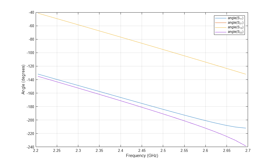
Compute its S-parameters using EM analysis and verify that the implemented phase shift is 90 degrees. A 90 degree phase shift is required to combine two outputs of the antenna.
sparamPhaseShift=sparameters(phaseShift, (2205:24.5:2695)*1e6);
figure; rfplot(sparamPhaseShift,'angle');
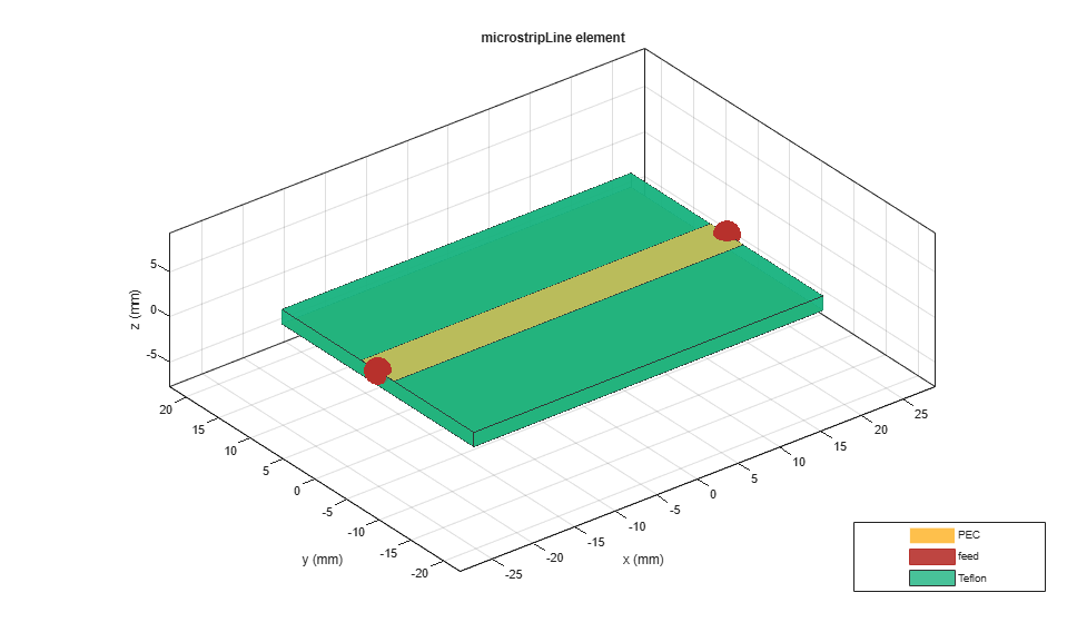
Design a microstrip line with the same length as the phase shifter to allow the other port of the Wilkinson splitter to reach the border of the board.
l1 = phaseShift.PortLineLength;
l2 = phaseShift.SectionShape.Length(2);
w = phaseShift.PortLineWidth;
mLine = microstripLine('Width',w, 'Length',2*(l1+w)+l2);
figure; show(mLine);
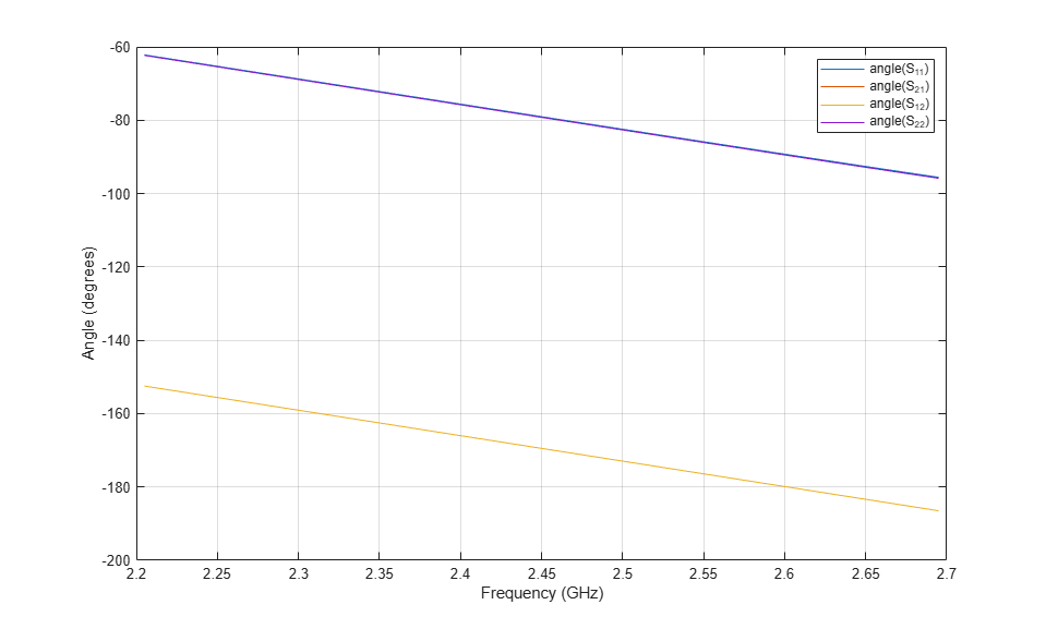
Calculate the S-parameters of the microstrip line.
sparamLine=sparameters(mLine, (2205:24.5:2695)*1e6);
figure; rfplot(sparamLine,'angle');
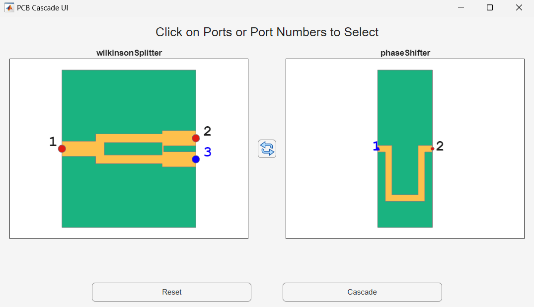
Connect the port 3 of the Wilkinson splitter with port 1 of the phase shifter using the pcbcascade object interactively.
Load the MAT file that contains wilkCombiner variable.
load varfile.mat
Run this command at the command line to create a cascaded object.
pcbcascade(wilkCombiner,phaseShift,'Interactive',true);
Select the port 3 of the Wilkinson splitter with port 1 of the phase shifter and then select the Cascade button.
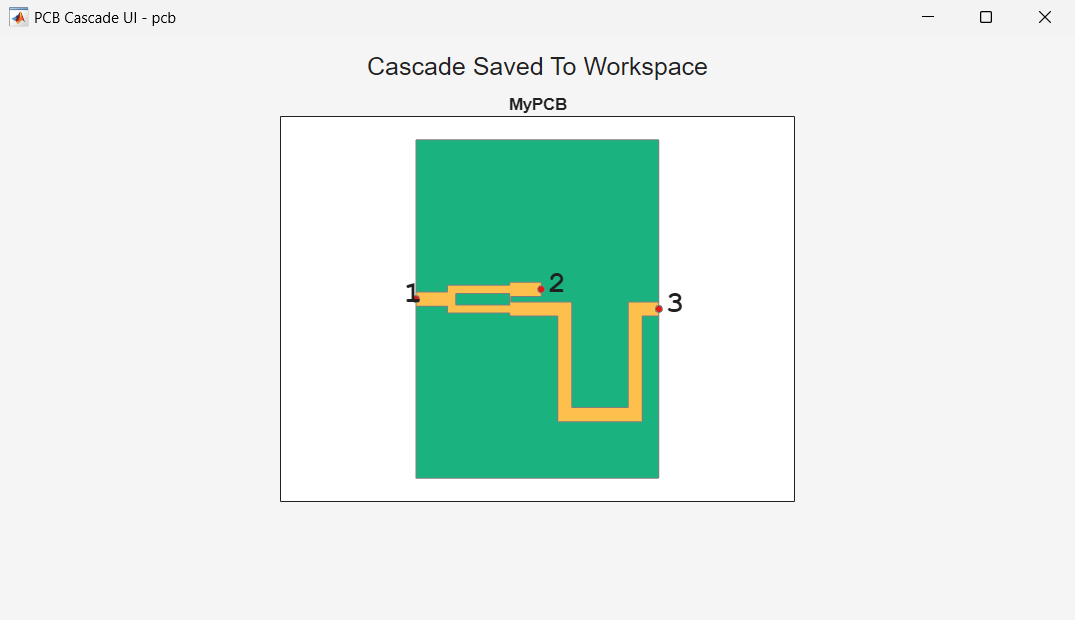
Save the cascaded object to the workspace with the name pcb by entering the variable name in Save to Workspace as field.
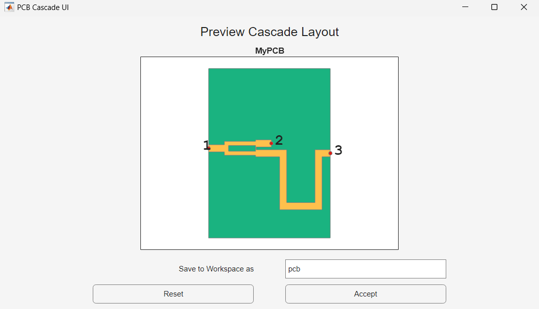
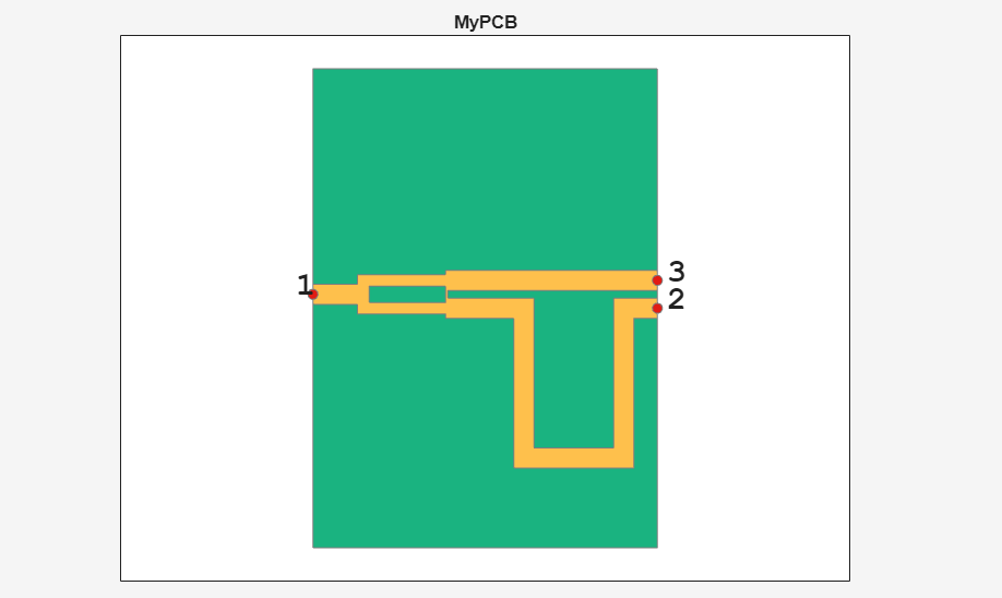
Visualize the cascaded object.
Connect port 2 of the cascaded PCB structure created in the previous step with port 1 of the microstrip line.
pcbcascade(pcb,mLine,'Interactive',true);
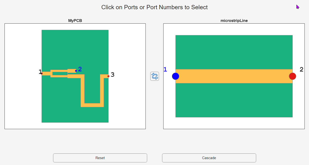
Save the resulting object to the workspace with the name pcb1.
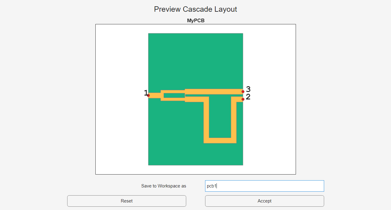
Visualize the cascaded object.
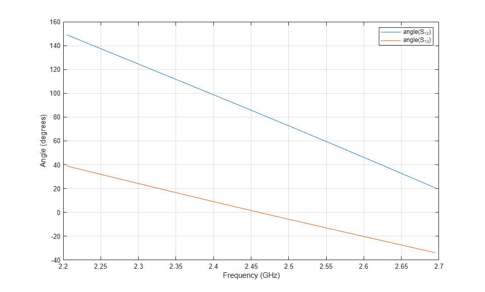
Use the EM analysis to compute the S-parameters of the PCB, save them in a Touchstone file. Verify the 90 degrees phase difference along the 2 branches.
sparamWilkSplitterPhaseShift=sparameters(pcb1, (2205:24.5:2695)*1e6);
figure; rfplot(sparamWilkSplitterPhaseShift,1,2,'angle');
hold on; rfplot(sparamWilkSplitterPhaseShift,1,3,'angle');
Export the data to a TouchStone file. rfwrite(sparamWilkSplitterPhaseShift,'wilkinsonSplitterPhaseShiftSparams.s3p')
Create the PCB integrating the Wilkinson combiner with the phase shift, the microstrip line. Compute the S-parameters and visualize them. Verify phase shifts on both branches as well as the transmission loss.
wilkSplitterPhaseShift = pcbcascade(wilkCombiner,phaseShift,3,1);
wilkSplitterPhaseShift = pcbcascade(wilkSplitterPhaseShift,mLine,2,1);
figure; show(wilkSplitterPhaseShift);
sparamWilkSplitterPhaseShift=sparameters(wilkSplitterPhaseShift, (2205:24.5:2695)*1e6);

figure; rfplot(sparamWilkSplitterPhaseShift,1,2,'angle');
hold on; rfplot(sparamWilkSplitterPhaseShift,1,3,'angle');
figure; rfplot(sparamWilkSplitterPhaseShift,1,2);
% rfwrite(sparamWilkSplitterPhaseShift,'wilkinsonSplitterPhaseShiftSparams.s3p')


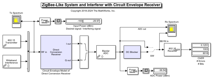
Update the Simulink model with the S-parameters of the PCB and run the simulation. Verify how the additional phase rotation introduced by the combiner / phase offset is accounted for in the baseband receiver.
Create the crossed dipole and analyze it using the sparameters function. And then input this antenna to the Antenna block. Open the resulting integrated model:
sobj = sparameters('SAW_Filter_Data.s2p');
open_system('RFReceiverWithPCB.slx')
w = warning('off','all');
sim('RFReceiverWithPCB.slx')
warning(w)
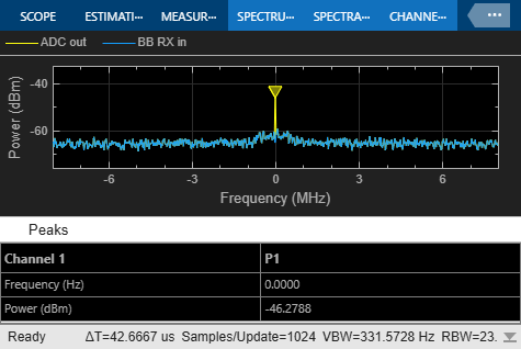
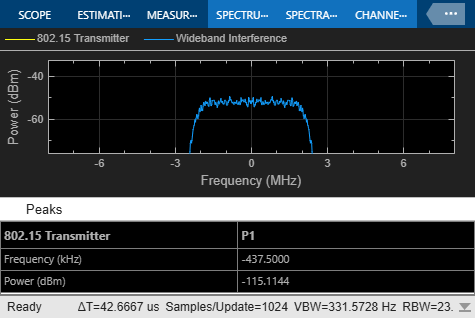
The model is not representative of the actual baseband receiver implementation, as the relative phase shift is normally recovered by means of an adaptive clock and phase recovery system. In this simple model, this approach could be used as the signal phase offset is constant and only dependent on the dispersive components in the chain. In the case of a wideband modulated signal though the phase shift would be frequency dependent, and the receiver would require an adaptive equalizer.
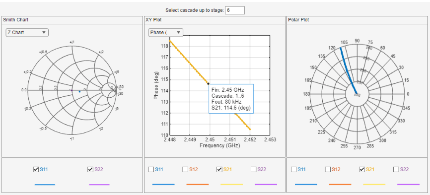
The implemented phase shift of 115 degrees has been determined by inspecting the phase rotation in the budget analysis. Run this command at the command line to open the RF Budget Analyzer app. Select the S-parameters plot button to plot the S-parameters plot. Enter 6 in Select cascade up to stage and observe the polar plot to see the phase shift of 115 degrees.
rfBudgetAnalyzer('rfbudget_RFReceiverXdipole.mat')