stripLineCustom
Create a coupled single-ended or differential transmission line in strip form
Since R2024b
Description
Use the stripLineCustom object to create edge-coupled striplines
located within the layers of multi-layer PCBs. Striplines are high speed transmission lines
used for routing various RF components in the inner layers of a multi-layer printed circuit
board (PCB). The structure consists of a transmission line trace surrounded by dielectric
material sandwiched between two ground planes.
Creation
Description
custstrip = stripLineCustom creates a default coupled form of
single-ended or differential transmission line. The default pcb substrate
isTeflon with a thickness of 0.0016 meters.
The resulting dimensions are for a default resonant frequency of 2.5
GHz.
custstrip = stripLineCustom(name=value) sets Propertiesusing one or more name-value arguments. For example
custstrip = stripLineCustom(TraceWidth=0.004) creates a custom
stripline with a trace width of 0.004 meters. Properties not
specified retain their default values.
Properties
Object Functions
show | Display PCB component structure or PCB shape |
sparameters | Calculate S-parameters for RF PCB objects |
mesh | Change and view mesh properties of metal or dielectric in PCB component |
current | Calculate and plot current distribution |
charge | Calculate and plot charge distribution |
feedCurrent | Calculate current at feed port |
layout | Plot all metal layers and board shape |
shapes | Extract all metal layer shapes of PCB component |
design | Design a custom transmission line in stripline form around a specified frequency |
rlgc | Compute resistances, inductances, conductances, and capacitances |
propagationDelay | Compute propagation delay of transmission line |
getZEven | Calculate even mode impedance of differential PCB transmission line |
getZOdd | Calculate odd mode impedance of differential PCB transmission line |
dgs | Create defected ground structure of PCB element |
Examples
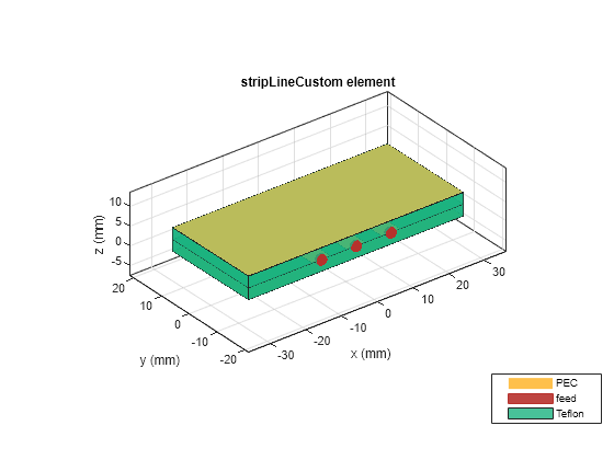
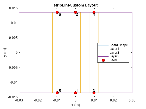
This example shows the creation and visualization of default custom stripline object
Create the stripline
Create the object
custline = stripLineCustom
custline =
  stripLineCustom with properties:

               TraceType: 'Single'
             TraceLength: 0.0271
              TraceWidth: 0.0051
            TraceOffsetX: 0
                  Height: 0.0030
       GroundPlaneLength: 0.0600
     LeftCoupledTraceGap: 0.0046
    RightCoupledTraceGap: 0.0046
               Substrate: [1×1 dielectric]
               Conductor: [1×1 metal]
Visualize the stripline
Use the show function and layout function to visualize the stripline
show(custline)
layout(custline)
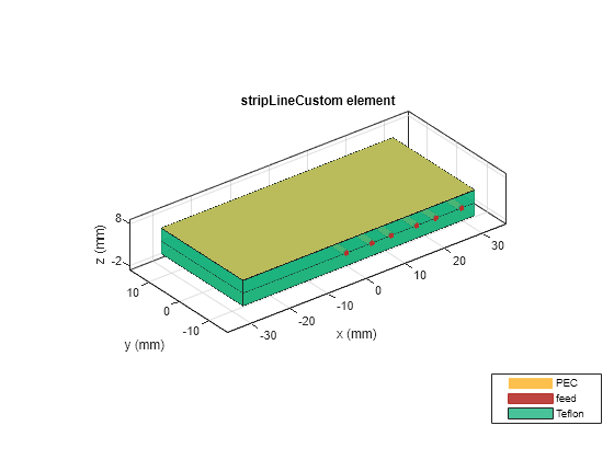
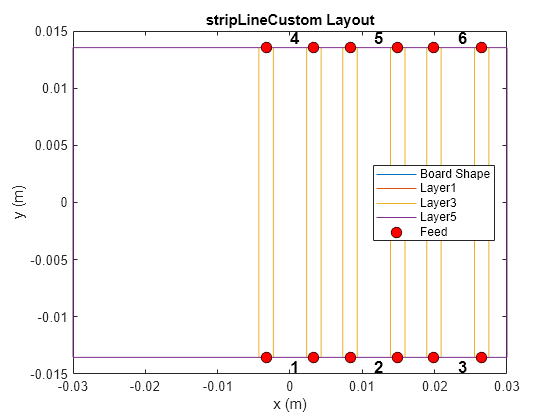
This example shows the creation and visualization of a differential stripline with two pairs of right-coupled lines.
Create Stripline
Set the appropriate stripline properties of the stripline object.
diffline = stripLineCustom(TraceType="Differential",TraceWidth=0.002,RightCoupledTraceGap=[0.003,0.003],LeftCoupledTraceGap=0)diffline =
stripLineCustom with properties:
TraceType: 'Differential'
TraceLength: 0.0271
TraceWidth: 0.0020
TraceSpacing: 0.0046
TraceOffsetX: 0
Height: 0.0030
GroundPlaneLength: 0.0600
LeftCoupledTraceGap: 0
RightCoupledTraceGap: [0.0030 0.0030]
Substrate: [1×1 dielectric]
Conductor: [1×1 metal]
Visualize Stripline
Use the show and layout functions to visualize the stripline.
show(diffline)
layout(diffline)
Version History
Introduced in R2024b