Matching Network Designer
Design, visualize, and compare matching networks for one-port load
Description
The Matching Network Designer app lets you design, visualize, and compare matching networks for one-port load.
Using this app, you can:
Design two- and three-component lumped element matching networks at desired frequencies and unloaded-Q factors.
Provide source and load impedance as a one-port Touchstone file, scalar impedance, RF circuit object, RF network parameter object, Antenna Toolbox™ object, or as an anonymous function.
Note
To load one-port circuit object to the app, you must set ports to your circuit object using the
setportsfunction.To use an Antenna Toolbox object, you must have an Antenna Toolbox license.
One-port Touchstone files include S1P, Z1P, and Y1P file types.
Sort the matching networks using constraints such as operating frequency range and power wave S-parameters.
Plot power wave S-parameters [1] of the matching network on a Smith™ chart and Cartesian plot.
Plot voltage standing wave ratio (VSWR) and impedance transformation plots.
Plot magnitude, phase, real, and imaginary parts of power wave S-parameters of the matching network.
Export selected networks as
circuitobjects or power wave S-parameters assparametersobjects.
Available Configurations
The app toolstrip contains these network configurations that you can use to design matching networks:
Pi-Topology
T-Topology
L-Topology
3-Components
Open the Matching Network Designer App
MATLAB® Toolstrip: On the Apps tab, under RF and Mixed-Signal, click the Matching Network Designer app icon.
MATLAB command prompt: Enter
matchingNetworkDesigner.
Examples
Type this command at the command line to open the Matching Network Designer app.
matchingNetworkDesigner
Select New under File section to start a new session. In the New Session window, specify the design requirements:
Zs Source —
Scalar Complex ImpedanceImpedance (Ohms) —
50+2i.Zl Load —
Touchstone FileFile Name —
dipole_example.s1pCenter Frequency —
1.5e9andBandwidth —
750e6.
The app only recognizes one-port Touchstone files and converts the center frequency and bandwidth to Hz.

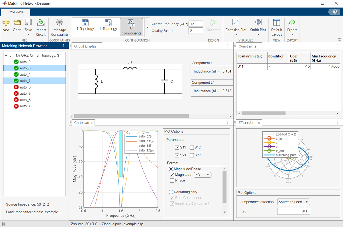
Select Start session. In the toolstrip of the app window, select 3-Components under the Configuration section and select Generate to generate the matching network. From the Matching Network Browser pane, select the nodes. For the purpose of this example, select auto_1. The Quality Factor is populated based on the data entered in the New Session window.

Set constraints to sort the three-component matching networks. To do this, click Manage Constraints. In the Design Constraints window, click ![]() button and add the constraints. Set the constraint to:
button and add the constraints. Set the constraint to:
abs(Parameter) — S11
Condition — <
Goal (dB) — –15
Min Frequency (GHz) — 1.4500
Max Frequency (GHz) — 1.5400
Weight — 1
Select Active and click OK.

The matching networks are sorted based on the constraints and the nodes are rearranged under the Matching Network Browser pane.

Compare the power wave S-parameter results between the nodes. For the purpose of this example, compare the power wave S-parameter results between auto_1 and auto_3 nodes. To do this, select the auto_1 and auto_3 nodes using the Ctrl key. The results are displayed in the Cartesian and Smith plot.

Deselect the auto_3 node. To visualize the impedance transformation of the auto_1 node, select Impedance Transformation under Smith Plot or select the ZTransform window on the right hand side of the app.

Design a narrow-band double tuning L-section matching network between a resistive source and a capacitive load in the form of a small monopole. This example designs an L-section matching network consisting of two inductors. The equivalent source impedance is 50 ohms and the load is a monopole with resonant frequency of around 1 GHz. The load (antenna) impedance is at 500 MHz, which is half the resonant frequency.
load_antenna = design(monopole,1e9);
sparams_load = sparameters(load_antenna,linspace(0.45e9,0.55e9,101));
To open the Matching Network Designer app, type this command at the command line.
matchingNetworkDesigner
Select New under File section to start a new session. In the New Session window, specify the requirements:
Zs Source —
Scalar Complex ImpedanceImpedance (Ohms) —
50Zl Source —
S-,Y-, or Z-parameter ObjectVariable Name —
sparams_loadCenter Frequency —
500e6andBandwidth —
10e6.
The app converts the center frequency and bandwidth to Hz.

Select Start Session. In the toolstrip of the app window, select L-Topology under Configuration section and select Generate to generate the matching network. From the Matching Network Browser pane, select the nodes. For the purpose of this example, select auto_1.

To plot the VSWR, select VSWR under Cartesian plot.

Design a pi-matching network with circuit objects. For the purpose of this example, the custom pi-matching network consists of two capacitors and an inductor.
Create a circuit object.
ckt = circuit('test_ckt2');Create two capacitors, C1 and C2 with the capacitance of 3.35 pF and 2.917 pF.
c1 = capacitor(3.35e-12,'C1');
c2 = capacitor(2.917e-12,'C2');
Create a 5.44 nH inductor.
l = inductor(5.44e-9,'L');Add C1 to the node [1,0] of the circuit object.
add(ckt,[1,0],c1);
Add L to the node [1,2] of the circuit object.
add(ckt,[1,2],l);
Add C2 to the node [2,0] of the circuit object.
add(ckt,[2,0],c2);
Save the circuit object.
save('test_file2.mat','ckt');
Set ports to the circuit object and resave the circuit object in MAT file type.
setports(ckt,[1 0],[2 0]);
save('test_file2.mat','ckt');
Type this command at the command line to open the Matching Network Designer app.
matchingNetworkDesigner
Select New under File section to start a new session. In the New Session window, specify the design requirements:
Zs Source —
Scalar Complex ImpedanceImpedance (Ohms) —
50Zl Source —
Touchstone FileFile Name —
dipole_example.s1pCenter Frequency —
1.5e9andBandwidth —
750e6
Select Import Circuit to import the custom pi-matching network designed in this example. Select node test_ckt2 under Matching Network Browser pane.

S11 and S21 plot of the custom pi-matching network is displayed under Cartesian plot.
Related Examples
Programmatic Use
Tips
Use this expression to set design constraints: |Parameter| Condition 10^(Goal (dB)/20). For example, |S21| > 10^(-3/20) implies that matching network circuits are sorted with
S21greater than -3dB as a design constraint. In linear scale the expression can be rewritten as |S21| > 0.7079.
Algorithms
References
[1] Kurokawa, K. “Power Waves and the Scattering Matrix.” IEEE Transactions on Microwave Theory and Techniques 13, no. 2 (March 1965): 194–202. https://doi.org/10.1109/TMTT.1965.1125964.
[2] Ludwig, Reinhold, and Gene Bogdanov. RF Circuit Design: Theory and Applications. Upper Saddle River, NJ: Prentice-Hall, 2009.
Version History
Introduced in R2021a