Sigma-Delta A/D Conversion
This example shows how to model analog-to-digital conversion by implementing a sigma-delta algorithm.
The oversampled sigma-delta A/D converter is a noise-shaping quantizer. The main purpose of noise shaping is to reshape the spectrum of quantization noise so that most of the noise is filtered out of the relevant frequency band such as the audio band for speech applications. The main objective is to trade bits for samples. That is, increase the sample rate but reduce the number of bits per sample. The resulting increase in quantization noise is compensated by a noise-shaping quantizer. This quantizer pushes the added quantization noise out of the relevant frequency band and thereby preserves a desired level of signal quality. This reduction in the number of bits simplifies the structure of A/D and D/A converters.
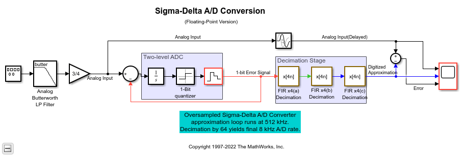
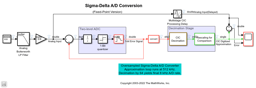
This example includes two models. In these models, the analog input is first prefiltered by an antialiasing prefilter whose structure is simplified because of oversampling. The input signal is oversampled by a factor of 64. The Integrator, 1-Bit Quantizer, and the Zero-Order Hold blocks comprise a two-level analog to digital converter (ADC). The output of the Zero-Order Hold block is then subtracted from the analog input. The feedback or approximation loop causes the quantization noise generated by the ADC to be highpass filtered, pushing its energy toward the higher frequencies (64*fs/2) and away from the relevant signal band.
The decimation stage reduces the sample rate back to 8 kHz. During this process, the decimation stage removes the high frequency quantization noise that was introduced by the feedback loop and removes any undesired frequency components beyond fs/2 (4 KHz) that were not removed by the simple analog prefilter.
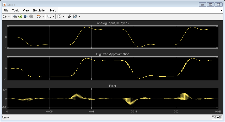
The Scope block shows the analog input signal, digitized approximation of the signal, and the error between the two signals. Open the models and run them. You will see that the digitized signal is a close approximation of the analog input signal.
Floating-Point Model
Open the model dspsdadc.slx using the open_system command.
Fixed-Point Model
Open the model dspsdadc_fixpt.slx using the open_system command.

Decimator Design
The two models in this example illustrate two possible decimator design solutions.
The floating-point version model uses a cascade of three polyphase FIR decimators. This approach reduces computation and memory requirements as compared to a single decimator by using lower-order filters. Each decimator stage reduces the sampling rate by a factor of four. The latency introduced by the filters is used to set the appropriate Time Delay parameter in the Transport Delay block. Due to the group delay of the filter, the three FIR Decimation blocks each introduce a latency of 16 samples. The actual value is 15.5 samples, which is rounded up to the nearest integer number of samples. Due to the decimation operation, the total latency introduced by the three filters is as follows: 16 (first filter) + 4*16 (second filter) + 16*16 (third filter) to give a final total delay of 336. The denominator of the Time delay parameter is the base rate of the model (512 kHz).
The fixed-point version uses a five-section CIC decimator to reduce the sampling rate by the same factor of 64. While not as flexible as a FIR decimator, the CIC decimator has the advantage of not requiring any multiplication operations. It is implemented using only additions, subtractions, and delays. Therefore, it is a good option in hardware implementations where computational resources are limited. The CIC Decimation introduces a latency of 158 samples, which is the group delay of the filter (157.5) rounded up to the nearest integer. This value is used in Time Delay parameter of the Multistage CIC Processing Delay block.
References
[1] Orfanidis, S. J. Introduction To Signal Processing, Prentice Hall, 1996.
See Also
Signal Generator (Simulink) | Analog Filter Design | FIR Decimation | CIC Decimation | Integrator (Simulink) | Sign (Simulink) | Zero-Order Hold (Simulink) | Transport Delay (Simulink) | Scope (Simulink)