Hauptinhalt

ProbeFeed

R2026b

Create a probe feed

Since R2024b

    Description

    Use the ProbeFeed object to specify the FeedDefinitions property in a parent pcbComponent object.

    The ProbeFeed object models a vertical conductive pin or via that excites the PCB by connecting a signal layer to a reference ground.

    Creation

    Description

    f1 = ProbeFeed creates a default ProbeFeed object.

    f1 = ProbeFeed(PropertyName=Value) sets object properties using one or more name-value arguments. PropertyName is the property name, and Value is the corresponding value. You can specify several name-value arguments in any order as PropertyName1=Value1,...,PropertyNameN=ValueN. Properties that you do not specify retain their default values.

    example

    Properties

    expand all

    Location to center the via, specified as a 1-by-2 vector in meters. The first and the second elements correspond to the X- and Y-coordinates in meters, respectively.

    The via center usually lies within a metal region on both the signal layer and the ground layer. If ViaModel is "strip", then the via center can also lie on the edge of one or both metal layers.

    Example: [0.2 0]

    Data Types: double

    Layer index for positive excitation site, specified as a positive integer scalar. SignalLayers is the layer index into the pcbComponent layer stack identifying the layer that the feed via reaches from the GroundLayer layer. Only the via terminus lies on this layer.

    Example: 2

    Data Types: double

    Layer index for negative excitation site, specified as a positive integer scalar. GroundLayers is the layer index into the pcbComponent layer stack. The ProbeFeed applies excitation at the GroundLayer layer in such a way that the positive signal propagates up the via towards the SignalLayer layer while the negative signal propagates outwards in the GroundLayer layer.

    Example: 4

    Data Types: double

    Cross-sectional shape of the via to construct, specified as one of the following:

    • "square" — Square shape

    • "hexagon" — Hexagonal shape

    • "strip" — Rectangular strip shape

    • "octagon" — Octagonal shape

    Example: "strip"

    Data Types: string

    Diameter of the via, specified as a positive scalar in meters.

    Example: 0.002

    Data Types: double

    Examples

    collapse all

    This example shows how to configure a probe feed object for a pcbComponent.

    Create a microstrip patch antenna using a pcbComponent object.

    r1 = traceRectangular('Length', 0.075, 'Width', 0.0357);
    r2 = traceRectangular('Length', 0.150, 'Width', 0.0750);
    d = dielectric('Air');
    p = pcbComponent;
    p.BoardShape = r2;
    p.BoardThickness = d.Thickness;
    p.Layers = {r1, d, r2};

    To expose the FeedDefinitions property set the FeedLocations property to FeedDefinitions, and assign a ProbeFeed object to that property.

    p.FeedFormat = 'FeedDefinitions';
    f = ProbeFeed('SignalLocations', [-0.0187 0], 'SignalLayers', 1, 'GroundLayers', 3, 'ViaDiameter', 0.001, 'ViaModel', 'square');
    p.FeedDefinitions = f;

    Show the structure, then calculate and plot its S-parameters over a frequency band.

    figure; show(p);
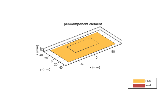
    Figure contains an axes object. The axes object with title pcbComponent element, xlabel x (mm), ylabel y (mm) contains 7 objects of type patch, surface. These objects represent PEC, feed.

    s = sparameters(p, linspace(1e9, 5e9, 51));
    figure; rfplot(s);
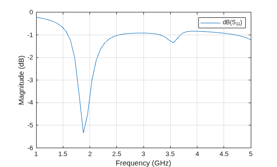
    Figure contains an axes object. The axes object with xlabel Frequency (GHz), ylabel Magnitude (dB) contains an object of type line. This object represents dB(S_{11}).

    Version History

    Introduced in R2024b

    See Also

    Objects

    Topics