Prototype IP Core on RFSoC with FPGA I/O
This example shows how to implement a quadrature phase shift keying (QPSK) wireless communication algorithm on the AMD® Zynq® UltraScale+™ ZCU216 evaluation kit or the Xilinx Zynq UltraScale+ ZCU111 evaluation kit. You generate HDL code for your algorithm, build and deploy the HDL design on an RFSoC device, and run a MATLAB® script to interactively capture data from the deployed HDL design.
Prerequisites
Install and configure these support packages and third-party tools:
HDL Coder™ Support Package for AMD® FPGA and SoC Devices.
Xilinx Vivado®. Use version in HDL Language Support and Supported Third-Party Tools and Hardware.
MathWorks® firmware image on the SD card of the board. See Guided Hardware Setup for AMD Boards.
Set Up Hardware Board
Set up the Xilinx Zynq UltraScale+ ZCU216 evaluation kit using these board connection settings. This example uses Tile0 and CH0 for both the ADC and DAC interfaces.
Connect DAC Tile-0 Ch-0 (P) to J42 connector.
Connect DAC Tile-0 Ch-0 (N) to J41 connector.
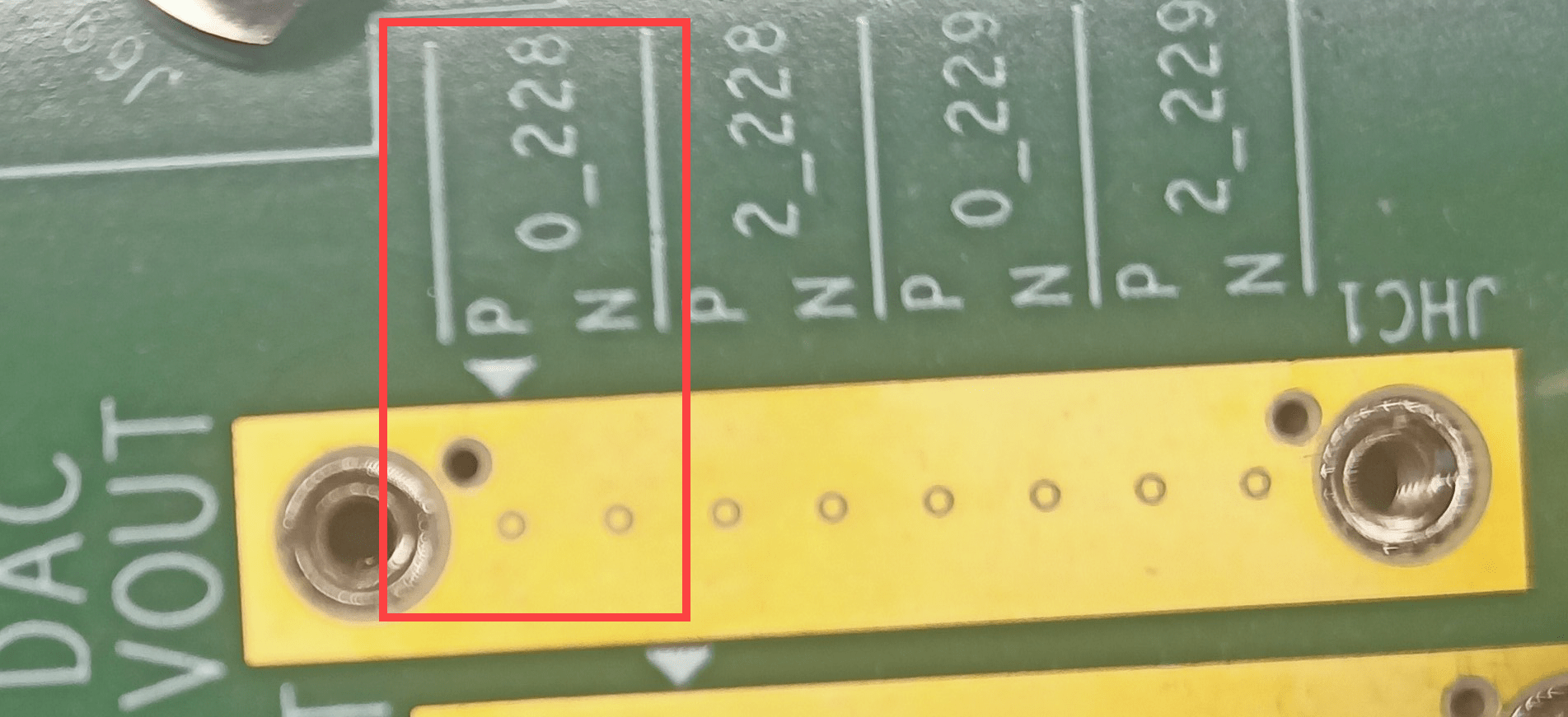
Connect ADC Tile-0 ch-0 (P) to J18 connector port.
Connect ADC Tile-0 ch-0 (N) to J16 connector port.

Connect the J40 and J17 connectors to create a loopback between the DAC and ADC interfaces.
Generate HDL IP Core and Bitstream
Open the example project and copy the example files to a temporary directory.
1. Navigate to the RFSoC root example directory of the HDL Coder Support Package for AMD FPGA and SoC Devices by entering these commands at the MATLAB command window.
example_root = (hdlcoder_rfsoc_examples_root)
cd (example_root)
2. Copy the example files in the QPSK folder to a temporary directory.
The hdlcoder_QPSKTxRx_RFSoC model is communication system that modulates data using the QPSK technique. The model transmits and receives real-time information.
open_system('hdlcoder_QPSKTxRx_RFSoC');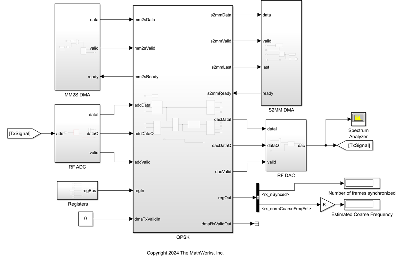
For more information, see Prototype IP Core on Zynq with MATLAB FPGA I/O Host Interface.
3. Set up the Xilinx tool path by using the hdlsetuptoolpath function. Use your own Xilinx Vivado installation path when executing the command.
>> hdlsetuptoolpath('ToolName','Xilinx Vivado','ToolPath',vivadopath);
4. Open the HDL Workflow Advisor. Right-click the QPSK subsystem and select HDL Code > HDL Workflow Advisor.
5. In the left pane, click 1. Set Target > 1.1. Set Target Device and Synthesis Tool, and set Target workflow to IP Core Generation and Target platform to Xilinx Zynq UltraScale+ RFSoC ZCU216 Evaluation Kit.
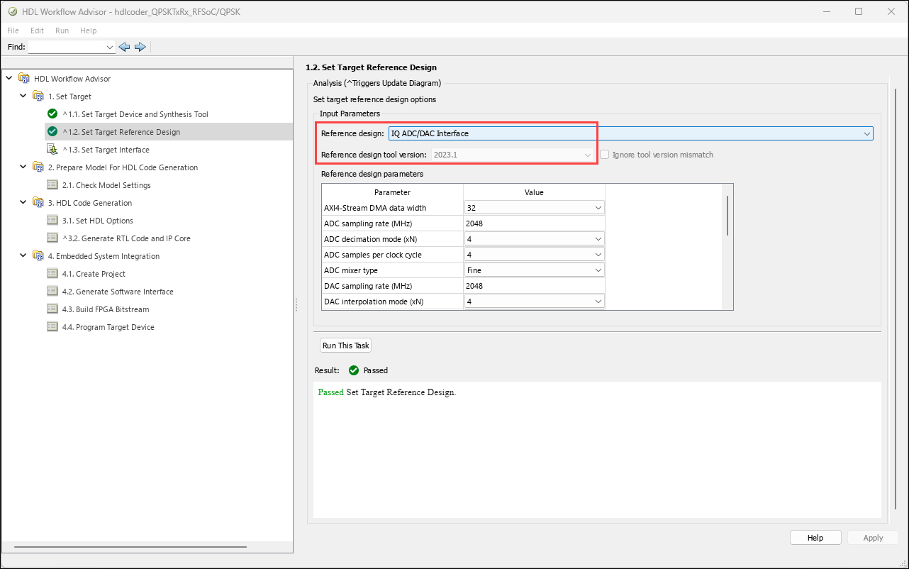
6. In the left pane, click 1. Set Target > 1.2. Set Target Reference Design, and set Reference design to I/Q ADC/DAC Interface. Because this algorithm is 32 bits, in the Reference design parameters section, set AXI4-Stream DMA data width to 32. Use the parameters settings mentioned in Reference design parameter table.
If you are using a Xilinx Zynq UltraScale+ RFSoC ZCU111 evaluation kit use these settings:
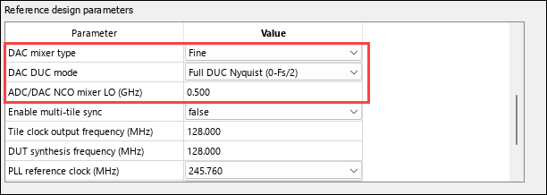
For more information on using these parameter values, see Host Interface Script Data Capture from Polyphase Channelizer Algorithm on RFSoC device.
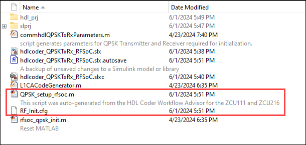
Right-click task 1.2 Set Target Reference Design and click Run to Selected Task. This step generates the QPSK_setup_rfsoc.m script and RF_Init.cfg files in your working directory. The QPSK_setup_rfsoc.m file lists the design specifications. You can edit QPSK_setup_rfsoc.m as per your design specifications and run the script before programming the target hardware. The RF_Init.cfg is non-editable configuration file that the RF tool uses to set the RF parameters that program the targeted hardware.
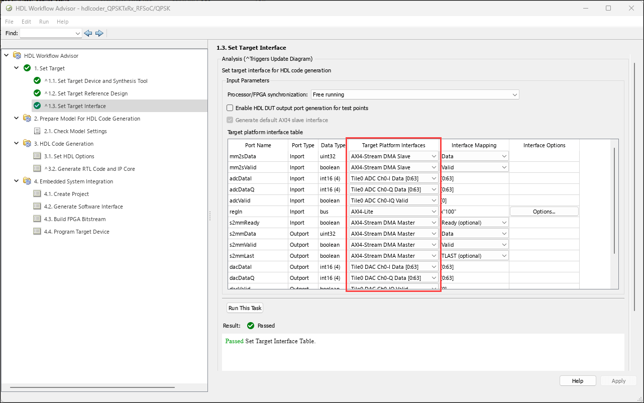
7. Click 1.3 Set Target Interface, and view the target interface mapping in the Target platform interface table. The Workflow Advisor automatically maps the DUT signals to the interface signals in the reference design.
HDL Workflow Advisor maps the input port mm2sData to AXI4-Stream DMA Slave and output port s2mmData to AXI4-Stream DMW Master and sets their data types to uint32. Therefore, the AXI4-Stream data width reference design parameter is set to 32 bit.
This example uses Tile0 and Ch0 to send data from the FPGA to the ADC and to retrieve the data from the DAC to the FPGA. This examples uses the same tiles for both the ADC and DAC. If you choose different tiles for the ADC and DAC, ensure the tiles and channels in the Target platform interface table section match the loopback connections on the hardware.
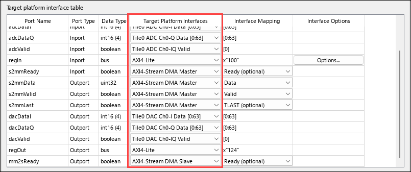
8. Run all the HDL Workflow Advisor tasks through step 3.2 Generate RTL Code and IP Core to generate the HDL code for the IP core.
Integrate the IP Core into the Xilinx Vivado Environment
1. To integrate HDL Coder IP into the embedded system, in the left pane of the HDL Workflow Advisor, click 4. Embedded System Integration > 4.1 Create Project. Click Run This Task. HDL Workflow Advisor creates a Xilinx Vivado project, generates an IP integrator embedded design, and provides links to the Vivado project in the task log.
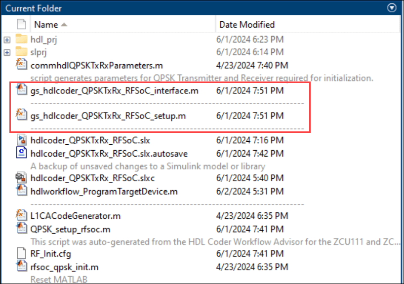
2. In step 4.2 Generate Software Interface, select Generate host interface script. Clear the Generate Simulink software interface model option and then click Run This Task. This step generates two MATLAB files, gs_hdlcoder_QPSKTxRx_RFSoC_setup and gs_hdlcoder_QPSKTxRx_RFSoC_interface, in your current folder. You can use these files to prototype your generated IP core directly from MATLAB. In this example, you use the host interface script to communicate with the hardware.
3. Click 4.3. Build FPGA Bitstream. To continue using MATLAB while building the bitstream file, click Run build process externally. Next, click Run This Task. Wait until the external shell displays a successful bitstream build.
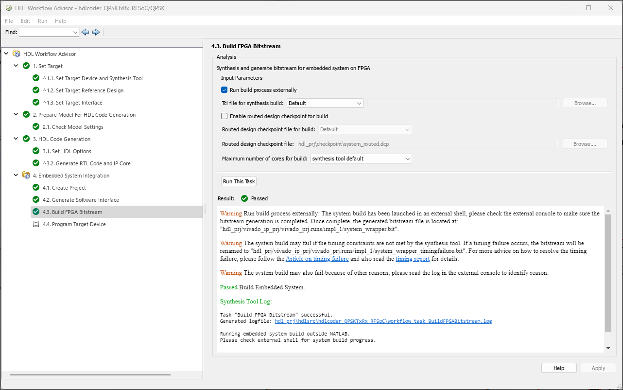
4. You can program the target device connected to your host machine either by running step 4.4 Program Target Device or by running the hdlworkflow_ProgramTargetDevice.m script generated in your working directory in step 4.3.
Visualize Data Using MATLAB Host Computer
Open the generated host interface script file.
open gs_hdlcoder_QPSKTxRx_RFSoC_interface.m
Modify the host interface script to:
Create a hardware object to establish a connection to your FPGA.
Write input control signals and stream the signals to the PS.
Read the output stream signals from the PS.
By default, the write and read frame length parameters are set to 1024 in the gs_hdlcoder_QPSKTxRx_RFSoC_setup script. This example uses the write and read frame length of 70.
To transmit and receive the streaming data using a MATLAB host, modify the host interface script gs_hdlcoder_QPSKTxRx_RFSoC_interface.m to:
Specify the board credentials such as, IP address, username, and password.
Set the DUT register values by using
writePortcommand.Print transmitted and received data on the MATLAB Command Window.
%--------------------------------------------------------------------------
% Host Interface Script
%
% Generated with MATLAB 24.2 (R2024b) at 21:18:21 on 03/04/2024.
% This script was created for the IP Core generated from design 'hdlcoder_QPSKTxRx_RFSoC'.
%
% Use this script to access DUT ports in the design that were mapped to compatible IP core interfaces.
% You can write to input ports in the design and read from output ports directly from MATLAB.
% To write to input ports, use the "writePort" command and specify the port name and input data. The input data will be cast to the DUT port's data type before writing.
% To read from output ports, use the "readPort" command and specify the port name. The output data will be returned with the same data type as the DUT port.
% Use the "release" command to release MATLAB's control of the hardware resources.
%--------------------------------------------------------------------------
rfsoc_qpsk_init; % Initialize the model parameters

%% Program FPGA
% Uncomment the lines below to program FPGA hardware with the designated bitstream and configure the processor with the corresponding devicetree.
% MATLAB will connect to the board with an SSH connection to program the FPGA.
% If you need to change login parameters for your board, using the following syntax:
% hProcessor = xilinxsoc(ipAddress, username, password);
hProcessor = xilinxsoc('192.168.1.101','root','root');

%% Create fpga object
hFPGA = fpga(hProcessor);

%% Setup fpga object
% This function configures the "fpga" object with the same interfaces as the generated IP core
gs_hdlcoder_QPSKTxRx_RFSoC_setup(hFPGA);
%% Write/read DUT ports
% Uncomment the following lines to write/read DUT ports in the generated IP Core.
% Update the example data in the write commands with meaningful data to write to the DUT.
%% AXI4-Lite

writePort(hFPGA, "regIn.tx_enable", 1); % One for sending valid data bits to SDR
writePort(hFPGA, "regIn.rx_reset_cs", 0);
writePort(hFPGA, "regIn.rx_src_sel", 1);  % Zero for internal loopback and one for SDR transmission

writePort(hFPGA, "regIn.capture_length", 70); % AXI4 Stream write frame length
writePort(hFPGA, "regIn.capture_src_sel", 0); % Zero for seeing data after QPSK and one for seeing data before QPSK
writePort(hFPGA, "regIn.capture_start", 1); % One to start capturing data from QPSK Rx

writePort(hFPGA, "regIn.tx_output_gain", 1);
writePort(hFPGA, "regIn.rx_input_gain", 1);
writePort(hFPGA, "regIn.capture_mode", 1);
fprintf('\n')
fprintf('####### Transmited Data #######\n')
msgNum = 0;
msg = sprintf('Hello world %d!\n',msgNum);

% Format Tx payload data
txDataBytes = uint8(zeros([1 dataBytesPerPacket]));
txDataBytes(1:length(msg)) = msg;
txDataU32 = typecast(txDataBytes,'uint32');
pause(0.1);


%% AXI4-Stream Read
writePort(hFPGA, "mm2sData", txDataU32);
%% AXI4-Stream Write
[rxData,rxValid] = readPort(hFPGA, "s2mmData");
fprintf('%s\n',char(rxBytes));
if rxValid
    disp('####### Rx Decoded Bytes #########');
    rxBytes = typecast(rxData.','uint8');
    fprintf('%s\n',char(rxBytes));
    idx = 1;
    for ii=1:numel(rxBytes)
        fprintf('%02X ',rxBytes(ii));
        if idx==16
            fprintf('\n');
            idx=1;
        else
            idx=idx+1;
        end
    end
    fprintf('\n');

else
    disp('####### Error: DMA read failed');
end
%% Release hardware resources
release(hFPGA);
delete(hFPGA);
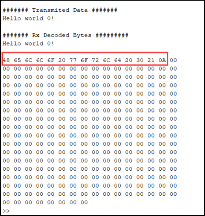
Run gs_hdlcoder_QPSKTxRx_RFSoC_interface.m. You can view transmitted and received message strings in the MATLAB Command Window. You can also customize the interface script to represent the received message string in hexadecimal form.
When you alter the hardware board connections physically, reset the IP Core by using the following command:
hFPGA.writeMemoryOffset("AXI4-Lite", 0x0,uint32(1))
You can also include the above command in the interface script gs_hdlcoder_QPSKTxRx_RFSoC_interface.m and re-run the interface script:
hFPGA.writeMemoryOffset("AXI4-Lite", 0x0,uint32(1)) % Reset the IP Core

writePort(hFPGA, "regIn.tx_enable", 1); % One for sending valid data bits to SDR
writePort(hFPGA, "regIn.rx_reset_cs", 0);
writePort(hFPGA, "regIn.rx_src_sel", 1);  % Zero for internal loopback and one for SDR transmission