Deploy a Real-Time Video Frame Accumulator by Using External Memory
In video processing designs, delaying entire frames is often necessary for algorithms such as temporal accumulation, motion estimation, or multi-frame noise reduction. However, storing full frames internally in a field-programmable gate array (FPGA) can quickly exceed the available on-chip memory, such as block random-access memory (RAM), especially when working with high-resolution video formats. To address this, you can offload delayed frames to external memory.
In this example, you create a recursive frame accumulator for 720p video on a Zynq®-based FPGA using HDL Coder. You use frame-to-sample optimization to convert a frame-based model into a pixel-streaming architecture, which you deploy in real-time by using AXI4-Stream Video interfaces.
To run this example, install and set up this software and hardware:
HDL Coder Support Package for AMD® FPGA and SoC Devices.
Xilinx® Vivado®. To view the supported versions, see HDL Language Support and Supported Third-Party Tools and Hardware.
Xilinx Zynq ZC706 Evaluation Kit.
Open and Examine the Model
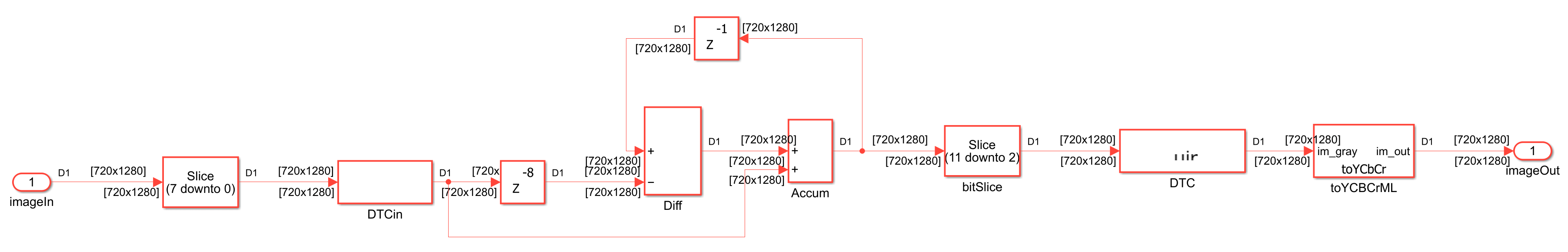
Open the hdlFrameAccumulator model. The DUT subsystem models a frame accumulator that computes the output using the complete frame at each time step. The model uses a recursive temporal filter that enhances motion by comparing the current frame to a delayed frame and accumulating the result over time.
load_system("hdlFrameAccumulator");
open_system("hdlFrameAccumulator/DUT");
set_param("hdlFrameAccumulator","SimulationCommand","Update");
To observe the algorithm, simulate the model for four seconds by clicking the Run button in the Simulation tab of the Simulink® Toolstrip. The test video features a triangle moving diagonally across the frame. The output shows a motion trail effect, where the triangle leaves a fading path behind it. This trail corresponds to the number of frames accumulated. In this image, the first and eighth frames of the input video zigzag_triangle_return_video.mp4 are shown on the left , and the processed output first and eight frames are shown on the right. Note that the eight previous triangle locations can be seen in the trail shown in eight output frame. The video frame size is 720-by-1280 pixels.
Processing entire frames on FPGAs and ASICs with limited I/O can require more resources than are typically available. For large frames, sample-based processing conserves memory, and reduces I/Os and latency. However, implementing even simple algorithms at the sample level requires you to design line buffers, state machines, and external memory controllers to manage the ring buffers and align multiple data streams. This process becomes more challenging as the design complexity increases.
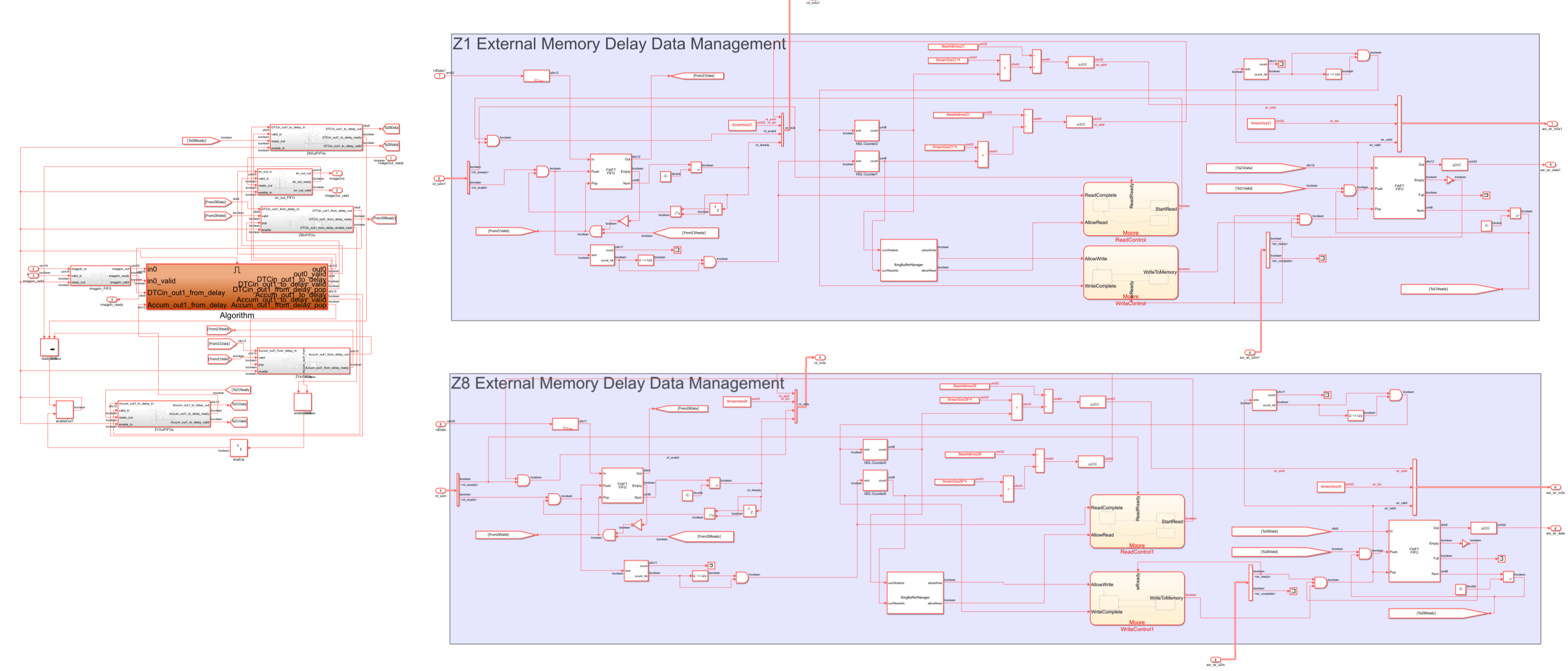
For example, if you want to model the frame accumulator implemented in the hdlFrameAccumulator model by using a sample-based approach, you must create these supporting elements manually. You can see an example of this method in the image below, which shows a model that implements the same video frame accumulator at the pixel level for a frame size of 24-by-32 to enable faster simulation. Because Simulink processes only one pixel per time step, simulating large frames can be slow. In this model, the orange subsystem contains the arithmetic logic for accumulation, while the remaining blocks contain the logic for data management.
You can address these challenges by using the frame-to-sample optimization to generate HDL code directly from the hdlFrameAccumulator model. With this approach, you can use simple adders and delay blocks in your design. HDL Coder generates the required buffering, external memory management, and AXI4 interface logic based on your configuration and reference design. Because Simulink processes entire frames, rather than individual pixels at each time step, the resulting model also simulates faster.
Enable Frame-to-Sample Optimization
First, optimize the model by using the frame-to-sample conversion:
1. Enable frame-to-sample conversion for the hdlFrameAccumulator model:
hdlset_param("hdlFrameAccumulator","FrameToSampleConversion","on");
2. Enable the HDL block property ConvertToSamples for the input image to be streamed, imageIn:
hdlset_param("hdlFrameAccumulator/DUT/imageIn","ConvertToSamples","on");
3. In the HDL Code tab, click Settings ![]() . In the Configuration Parameter dialog box, select the Optimization pane, then select the Frame to Sample Conversion tab. You can use the Delay size threshold for external memory parameter to specify the minimum delay size, in kilobytes, to use for external mapping.
. In the Configuration Parameter dialog box, select the Optimization pane, then select the Frame to Sample Conversion tab. You can use the Delay size threshold for external memory parameter to specify the minimum delay size, in kilobytes, to use for external mapping.
In this example, each 720p video frame is 1280-by-720 pixels, 8 bits per pixel, which results in each frame being approximately 922 KB. Set the threshold to a value smaller than the smallest delay in the design. To map both delays to external memory, set the parameter value to a value smaller than the smallest delay in the design. For this example, set the threshold to 100 KB:
hdlset_param("hdlFrameAccumulator","DelaySizeThreshold", 100);
4. You can modify the size of the FIFOs that control the streaming of the input, output, and external delays. In the Configuration Parameters dialog box, in the Frame to Sample Conversion tab, set the values of the Input FIFO size and Output FIFO size parameters. For real-time processing, allocate enough space to buffer one or two full lines of pixel data. To buffer two lines at 1280 pixels per line, set each FIFO size to 2560:
hdlset_param("hdlFrameAccumulator","InputFIFOSize", 2560);
hdlset_param("hdlFrameAccumulator","OutputFIFOSize", 2560);
5. Set up the Xilinx Vivado synthesis tool path by using the hdlsetuptoolpath command. Use your own Vivado installation path when you run the command.
hdlsetuptoolpath("ToolName","Xilinx Vivado","ToolPath",vivadopath);
6. In the HDL Code tab, in the Output section, set the drop-down button to IP Core.
7. Select the DUT subsystem which is the design under test (DUT) for this example. In the HDL Code tab, ensure that Code for is set to this subsystem. To remember the selection, you can pin this option.
Generate IP Core
This image shows how the HDL Coder Generated IP core integrates with the Default video system with External DDR3 Memory Access reference design available in the HDL Coder Support Package for AMD FPGA and SoC Devices. The IP core generated from the model, and the rest of the system is part of the predefined video reference design, which includes IP blocks for HDMI input and output, as well as access to external memory.
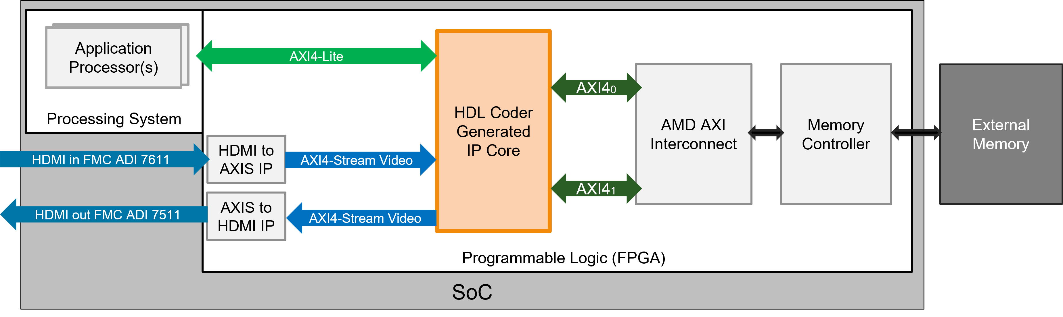
The IP core receives a video stream from the HDMI input IP, processes it, and sends the output stream to the HDMI output IP. The IP core transfers video data by using AXI4-Stream Video interfaces. The reference design also includes two AXI4 Master interfaces connected to a pre-configured AMD AXI interconnect and a memory controller, which enables access to external memory. The IP core clock derives from the HDMI clock, which runs at 74.25 MHz for 720p HDMI video.
Add Reference Design and Configure Model for Deployment
To add the Default video system with External DDR3 Memory Access reference design to your MATLAB® path, enter:
addpath(genpath(fullfile(hdlcoder_amd_examples_root,"ZC706")))Next, prepare the model for deployment by using the model configuration parameters.
1. In the HDL Code tab, click Settings ![]() to open the Configuration Parameters dialog box. Select the HDL Code Generation > Target pane.
to open the Configuration Parameters dialog box. Select the HDL Code Generation > Target pane.
2. Set Target Platform to Xilinx Zynq ZC706 evaluation kit, Reference Design to Default video system with External DDR3 Memory Access, and Target Frequency to 74.25.
3. Click OK.
Configure External Memory Access and Arbitration
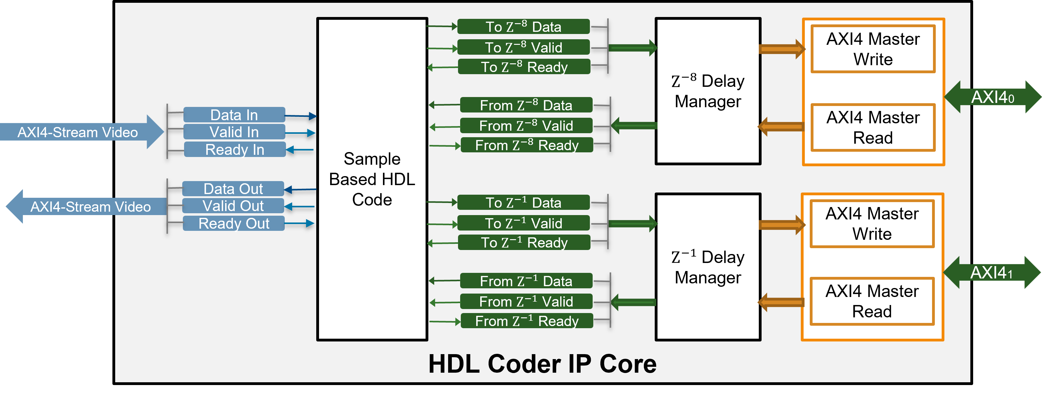
During code generation, HDL Coder transforms a frame-based algorithm into sample-based HDL code and generates additional data, valid, and ready ports to support streaming. For delays that exceed the specified Delay size threshold for external memory value, HDL Coder also inserts logic to offload them to external memory by using the same streaming protocol. The DUT Subsystem block, offloads two delays to external memory: one for the eighth frame design delay of the input, and another for the frame delay in the feedback loop. Each of these delays is managed through a pair of streaming interfaces. One interface is used to write the delay data out of the DUT, and another is used to read the delayed data back into the DUT. Both interfaces follow the standard streaming handshake protocol using data, valid, and ready signals. This image shows this transformation.
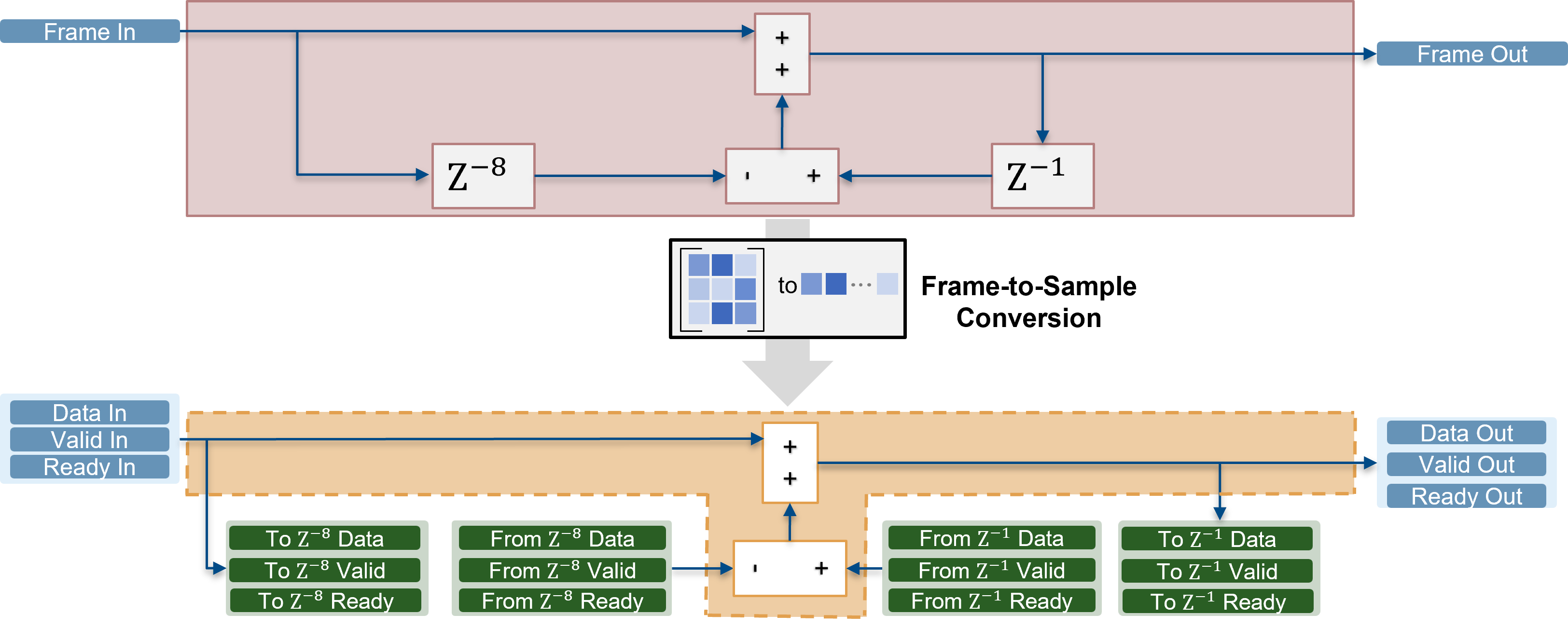
To use external memory resources such as DDR (Double Data Rate) memory on your FPGA board, the design must manage how data is stored and retrieved. Because DDR memory is optimized for burst transfers, during IP core generation, HDL Coder generates a frame manager that converts the sample-based data, valid, and ready interfaces of each delay into a memory protocol that supports burst reads and writes.
When your design includes multiple delays, in addition to protocol conversion, a mechanism for arbitration is required. Arbitration is the process of resolving simultaneous memory access requests from multiple sources so that only one transfer occurs at a time. You can manage memory access for multiple delays:
Shared Interface: A single AXI4 Master interface is exposed at the IP core boundary. HDL Coder generates an internal arbiter to manage access to external memory. Because only one AXI4 Master connection is required in the reference design, using this option simplifies integration.Independent Interfaces: A separate AXI4 Master interface is generated for each delay. Arbitration is handled externally in the reference design, which allows the arbitration logic to run at a higher clock frequency. This option is better suited for real-time applications, but requires you to handle the arbitration outside or your IP core.
When you generate HDL code, HDL Coder generates the arbitration logic inside the IP core or in the reference design, depending on the setting of the MemoryInterfaceForFrameDelay parameter.
Because this model represents a real-time model, you must configure the model to use independent interfaces for arbitration. To configure the model:
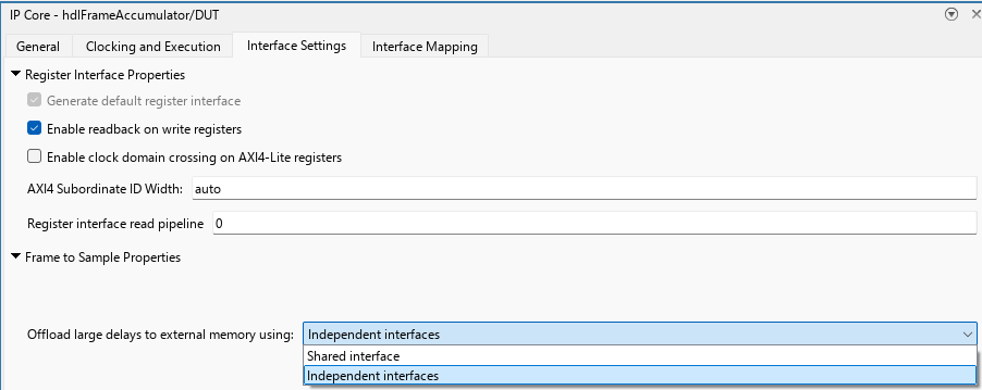
Open the IP Core pane. In the HDL Code tab, click Target Interface.
Select the Interface Settings tab. Under Frame to Sample Conversion Properties, set Offload Large Delays to External Memory using option to
Independent Interfaces.
HDL Coder generates a delay manager for each delay identified in the algorithm. For the hdlFrameAccumulator model, HDL Coder creates a delay manager for the input delay of size eight and a delay manager for the one frame accumulation delay. Each delay manager communicates with DDR by using an independent AXI4-Master interface.
Generate the IP core
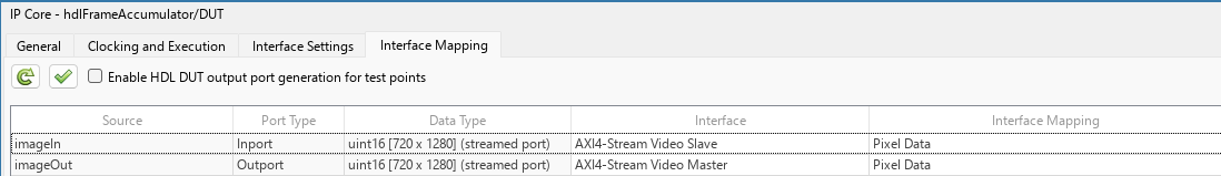
1. In the IP Core pane, select Interface Mapping pane to map your DUT ports to interfaces in the reference design.
2. To compile the model and populate the DUT ports and their data types, click the Reload button ![]() .
.
3. For the DUT port imageIn, set the Interface column to AXI4-Stream Video Slave. For the DUT port imageOut, set the Interface column to AXI4-Stream Video Master.
4. Validate your settings by clicking the Validate IP core settings and interface mapping button ![]() .
.
5. In the HDL Code tab of the Simulink Toolstrip, click Generate IP Core.
After IP core generation, HDL Coder produces a Code Generation Report. In the left pane, click IP Core Generation Report to view a summary of the generated IP core, interface mappings, and a detailed description of the frame management logic used to offload delays to external memory. The image shows the IP core generation report for the IP core generated for the hdlFrameAccumulator/DUT subsystem.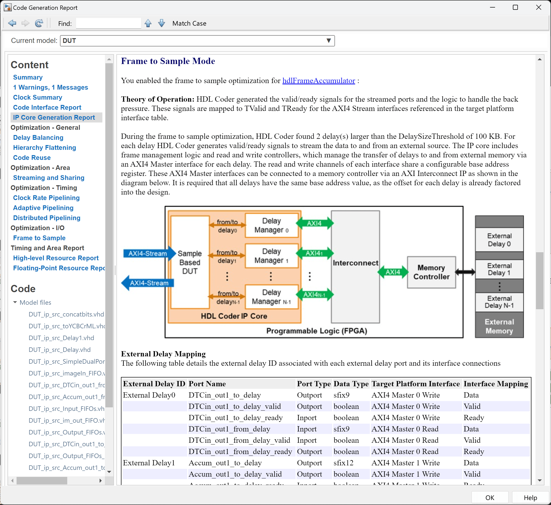
Deploy and Run Model on Xilinx Zynq ZC706 Evaluation Kit
To create a Vivado project and launch synthesis and implementation, in the HDL Code tab, click Build Bitstream. HDL Coder first inserts the generated IP core into the Default video system with External DDR3 Memory Access reference design, which uses:
A Xilinx AMD AXI interconnect to arbitrate the memory access of the two delays
A Xilinx Memory Interface Generator (MIG) IP to access the onboard DDR3 memory
HDMI input and output IP blocks to transfer video between the FMC card and the FPGA
Converters to convert between AXI4-Stream Video and HDMI
and then it runs synthesis and implementation on Vivado in an external window
Run Algorithm on External Hardware
When using the frame-to-sample conversion, the frame size in the DUT is fixed and inherited from the source video. After the external window indicates the bitstream has been generated, you can download the bitstream. In the HDL Code tab, select Build Bitstream > Program Target Device.
After programming the FPGA hardware, connect a 720p HDMI video source, such as the HDMI output of your computer, to the FMC HDMI input on the ZC706 board. Then connect a 720p-capable monitor to the FMC HDMI output. The system will begin processing video in real time. The image shows the setup, connections, and an image of the algorithm running on the ZC706 board with the test video as input. Notice that the live video result matches the Simulink simulation.
Performance Considerations
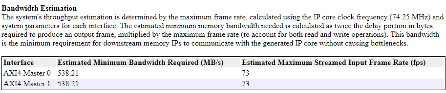
On the reference design, the Programmable Logic (PL) DDR controller is configured with a 64-bit AXI4-Slave interface running at 200 MHz, which provides a bandwidth of 1600 MB/s. In this example, the algorithm processes only the luma (Y) component of the YCbCr 4:2:2 video input, while the Cb and Cr components are held constant. Each delay stores 8-bit data, but the system uses a 32-bit AXI4 Master interface per delay. As a result, each delay element is padded with zeros before being written to external memory. Consequently, two AXI4 Master interfaces are connected to the DDR controller through an AMD AXI interconnect. You can find the estimated bandwidth requirement in the IP Core Generation Report for each AXI4 Master Channel. For this example, each channel requires approximately 538.21 MB/s when the system runs at 73 fps, which is within the available bandwidth of the memory controller.
For higher resolutions or frame rates, you may need to increase the IP core clock frequency by modifying the reference design, adjust Frame to Sample FIFO sizes to accommodate larger data sizes, and ensure the DDR memory controller and AMD AXI interconnect can sustain the required throughput.