Debug IP Core Using Hardware-Software Deployment
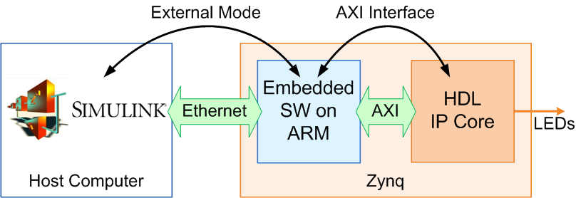
When you are prototyping and developing an algorithm for Zynq® platform, it is useful to monitor, tune, and debug the algorithm while it
runs on hardware. This example shows how to use features like external mode, AXI
interface and HDL FIFO blocks to probe into the Zynq design. Using the external mode feature, you can probe the internal data
in the software running on the ARM® processor. And because the ARM processor is connected to the FPGA through AXI interface, you can monitor
and tune the parameters on FPGA as well. Together with HDL FIFO blocks, you can capture
fast FPGA data and retrieve it back to Simulink® for analysis.
This example shows how to use features like external mode, AXI interface and HDL FIFO blocks to probe into the Zynq design, capture fast FPGA data, and retrieve it back to Simulink for analysis. You can also do similar monitoring with FPGA vendor tools like ChipScope™ or SignalTap™. But the strength of this approach is that you can get all the visualization benefits of Simulink, like various scope blocks, and you can also build your own custom controls, triggers, or qualifiers in Simulink.
Debug IP Core using Hardware-Software Deployment
Requirements
Xilinx® Zynq-7000 SoC ZC702 Evaluation Kit
HDL Coder Support Package for AMD FPGA and SoC Devices
Follow the Set up Zynq hardware and tools section in Get Started with IP Core Generation from Simulink Model to setup ZC702 hardware.
Example Model
Open the example model.
open_system('hdlcoder_data_capture');

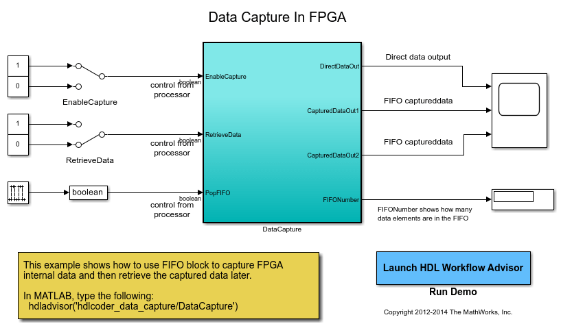
The subsystem DataCapture is the hardware subsystem targeting the FPGA fabric. Inside this subsystem, the OriginalDUT subsystem contains a Trigonometric Function block, which generates fast sine and cosine data streams. The OriginalDUT subsystem represents our algorithm design. If we want to debug this design, how do we capture and monitor this fast data stream?
The FPGA runs at a much faster clock frequency than the software code on the ARM processor. External mode can be used with the software running on the ARM processor to monitor slow-changing status parameters, such as FIFO status, but the sample rate of the software code, for example, 1KHz, is not fast enough to capture the fast-changing data in the FPGA, for example, 50MHz.
This example shows how to use a FIFO block to capture the fast FPGA data, and then use the software on the ARM processor to retrieve the captured data through the AXI interface and external mode.
For debugging purposes, we add the subsystem Debug_FIFOs to the DUT. This subsystem uses two HDL FIFO blocks to capture the fast data streams for future retrieval. The control signal inputs to the Debug_FIFOs subsystem are connected to the DUT interface, and are connected to the ARM processor via the AXI interface.
At the top level of the example model, when the EnableCapture switch is turned on, and RetrieveData switch is turned off, the Debug_FIFOs module will capture 1000 data samples into the HDL FIFO blocks. This is the data capture phase. Then, when the EnableCapture switch is kept on, and the RetrieveData switch is turned back on, the Debug_FIFOs module will transfer the captured data back to the ARM processor. This is the data retrieval phase. You can use the manual switches to switch between these two phases to capture and monitor the internal FPGA data.

Thus, for every signal you want to monitor, you can insert more Debug_FIFO modules to your design to capture and retrieve the data back to Simulink. You can also use your own control signals, or extend this example with your own triggers, or qualifiers.
The output port of the hardware subsystem, DirectDataOut, outputs data directly to the AXI interface. In contrast, the output ports CapturedDataOut1 and CapturedDataOut2 outputs captured data from the FIFOs. We will compare the results of these two outputs in the last section.
Deploy the Design on Zynq Hardware
Next, we will start HDL Workflow Advisor from the model and run through the Zynq HW/SW co-design workflow to deploy this design on Zynq hardware. For a detailed step by step guide, refer to the example Get Started with IP Core Generation from Simulink Model.
1. In the Set Target > Set Target Device and Synthesis Tool task, for Target workflow, select IP Core Generation. For Target platform, select Xilinx Zynq ZC702 evaluation kit. Run this task.
2. In the Set Target > Set Target Interface task, choose AXI4-Lite for all the input and output ports.

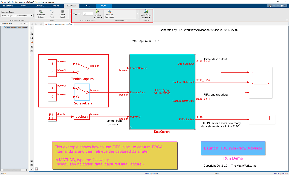
3. Then run through all the workflow steps to generate HDL IP, create an EDK project, generate the software interface model, and build and download the FPGA bitstream. The generated software interface model is shown in following picture:

4. Configure and build the software interface model for external mode:
In the generated model, click on Hardware pane and go to Hardware settings to open Configuration Parameter dialog box.
Select Solver and set Stop Time to inf.
From the Hardware pane, click the Monitor and Tune button.
Click the Run button on the model toolstrip. Embedded Coder builds the model, downloads the ARM executable to the Zynq ZC702 hardware, executes it, and connects the model to the executable running on the Zynq ZC702 hardware.
Capture and Display Data from Zynq Hardware
Now both the hardware and software parts of the design are running on Zynq hardware, the next step is to capture and retrieve data from the Zynq board.
Once the external mode is connected, make sure the EnableCapture switch is in the 1 position, and the RetrieveData switch is in the 0 position. Notice the FIFONumber display box increases to 1000 almost immediately. This means the FIFO inside the FPGA fabric started capturing data and was quickly filled with 1000 data samples.
Open the Time Scope block and observe the DirectDataOut output in the first row. Notice the received data is a seemingly random waveform between -1 and 1. This is because the FPGA is running at a much faster frequency than software is running on the ARM processor. Directly using external mode to monitor fast FPGA data means sampling a fast sine waveform at a very slow rate, which generates a random waveform between -1 and 1.
Now double-click the RetrieveData switch to enable data readout. The EnableCapture switch needs to be kept on. When the RetrieveData switch is turned on, the internal logic modeled in this example sends out the captured data samples one by one from FIFO to the ARM processor, through the AXI interface. These data samples are then sent from ARM processor to Simulink via external mode. Notice the FIFONumber display box decreases to 0.
Open the Time Scope block, the second and third row of the scope now shows the sine and cosine wave we captured in the FIFO. Following picture shows the scope waveforms.
