Run a Deep Learning Network on FPGA with Live Camera Input
This example shows how to model preprocessing logic that receives a live camera input. You implement it on a Zynq® Ultrascale+™ MPSoC ZCU102 board by using a custom video reference design that has an integrated deep learning processor IP core for object classification. This example uses the HDL Coder™ HW/SW co-design workflow. For this example, you need:
Deep Learning HDL Toolbox™
Deep Learning HDL Toolbox Support Package for Xilinx FPGA and SoC Devices
Deep Learning Toolbox™
HDL Coder™
Simulink™
Introduction
In this example, you:
Model the preprocessing logic that processes the live camera input for the deep learning processor IP core. The processed video frame is sent to the external DDR memory on the FPGA board.
Simulate the model in Simulink® to verify the algorithm functionality.
Implement the preprocessing logic on a ZCU102 board by using a custom video reference design which includes the generated deep learning processor IP core.
Individually validate the preprocessing logic on the FPGA board.
Individually validate the deep learning processor IP core functionality by using the Deep Learning HDL Toolbox™ prototyping workflow.
Deploy and validate the entire system on a ZCU102 board.
This figure is a high-level architectural diagram of the system. The result of the deep learning network prediction is sent to the ARM processor. The ARM processor annotates the deep learning network prediction onto the output video frame.

The objective of this system is to receive the live camera input through the HDMI input of the FMC daughter card on the ZCU102 board. You design the preprocessing logic in Simulink® to select and resize the region of interest (ROI). You then transmit the processed image frame to the deep learning processor IP core to run image classification by using a deep learning network.
Select and Resize the Region of Interest
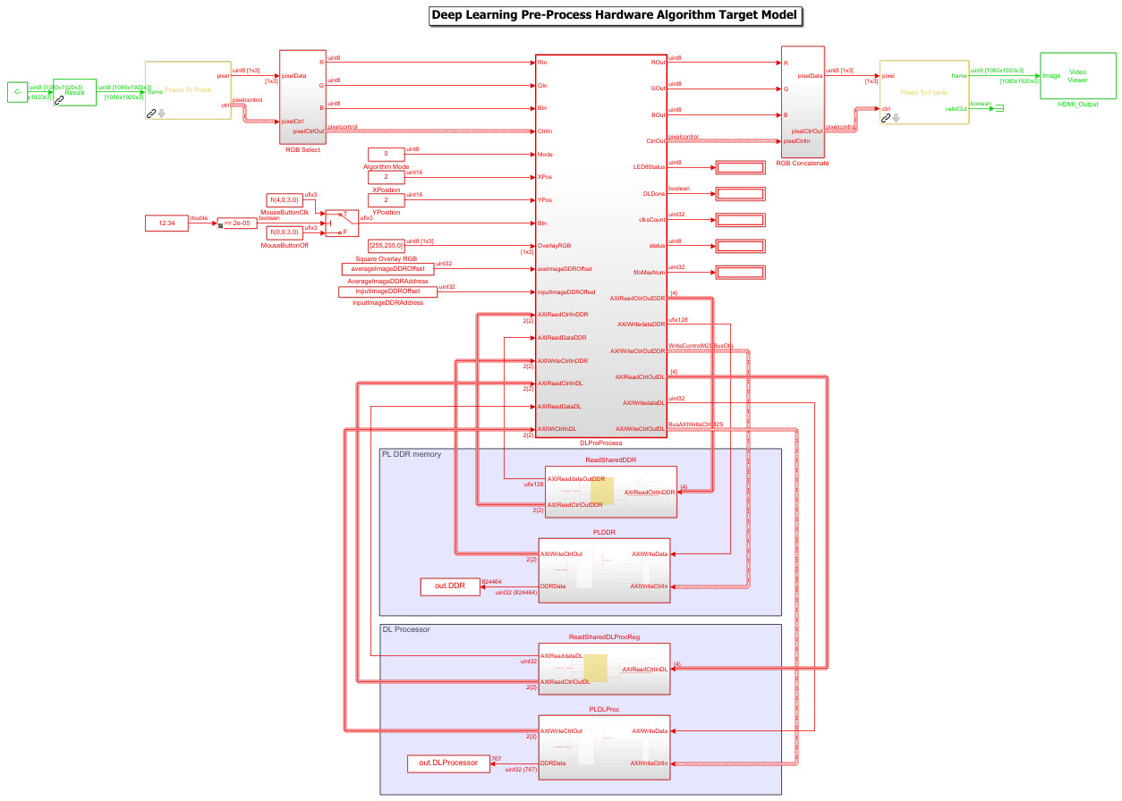
Model the preprocessing logic to process the live camera input for the deep learning network and send the video frame to external DDR memory on the FPGA board. This logic is modeled in the DUT subsystem:
Image frame selection logic that allows you to use your cursor to choose an ROI from the incoming camera frame. The selected ROI is the input to the deep learning network.
Image resizing logic that resizes the ROI image to match the input image size of the deep learning network.
AXI4 Master interface logic that sends the resized image frame into the external DDR memory, where the deep learning processor IP core reads the input. To model the AXI4 Master interface, see Model Design for AXI4 Master Interface Generation (HDL Coder).
This figure shows the Simulink® model for the preprocessing logic DUT.

Generate Preprocessing Logic HDL IP Core
To implement the preprocessing logic model on a ZCU102 SoC board, create an HDL Coder™ reference design in Vivado™ which receives the live camera input and transmits the processed video data to the deep learning processor IP core. To create a custom video reference design that integrates the deep learning processor IP core, see Authoring a Reference Design for Live Camera Integration with Deep Learning Processor IP Core.
Start the HDL Coder HDL Workflow Advisor and use the Zynq hardware-software co-design workflow to deploy the preprocessing logic model on Zynq hardware. This workflow is the standard HDL Coder workflow. In this example the only difference is that this reference design contains the generated deep learning processor IP core. For more details refer to the Get Started with IP Core Generation from Simulink Model (HDL Coder) example.
1. Start the HDL Workflow Advisor from the model by right-clicking the DLPreProcess DUT subsystem and selecting HDL Advisor Workflow.
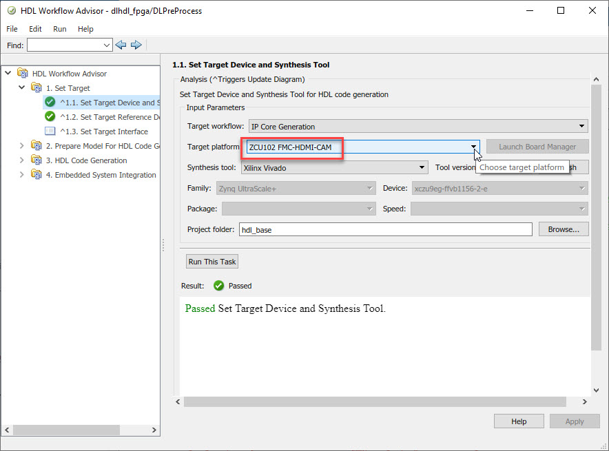
In Task 1.1, IP Core Generation is selected for Target workflow and ZCU102-FMC-HDMI-CAM is selected for Target platform.

In Task 1.2, HDMI RGB with DL Processor is selected for Reference Design.

In Task 1.3, the Target platform interface table is loaded as shown in the following screenshot. Here you can map the ports of the DUT subsystem to the interfaces in the reference design.

2. Right-click Task 3.2, Generate RTL Code and IP Core, and then select Run to Selected Task. You can find the register address mapping and other documentation for the IP core in the generated IP Core Report.
Integrate IP into the Custom Video Reference Design
In the HDL Workflow Advisor, run the Embedded System Integration tasks to deploy the generated HDL IP core on Zynq hardware.
1. Run Task 4.1, Create Project. This task inserts the generated IP core into the HDMI RGB with DL Processor reference design. To create a reference design that integrates the deep learning processor IP core, see Authoring a Reference Design for Live Camera Integration with Deep Learning Processor IP Core.
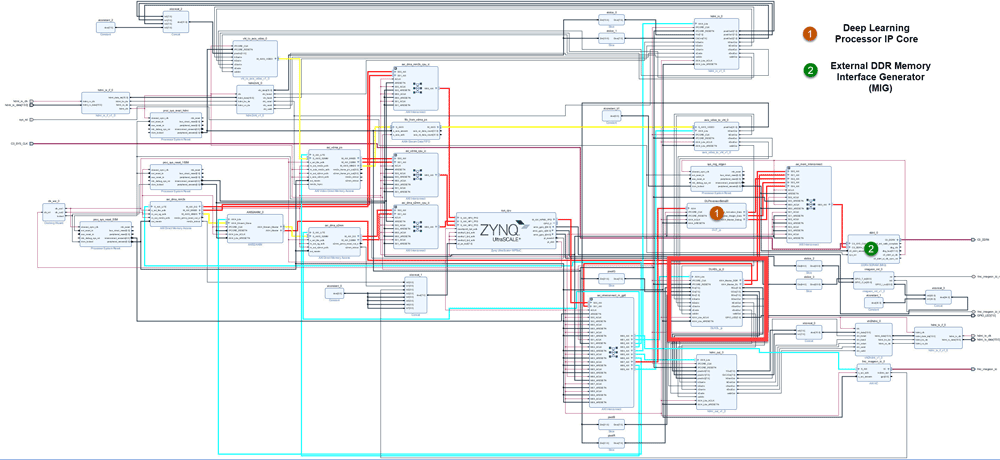
2. Click the link in the Result pane to open the generated Vivado project. In the Vivado tool, click Open Block Design to view the Zynq design diagram, which includes the generated preprocessing HDL IP core, the deep learning processor IP core and the Zynq processor.

3. In the HDL Workflow Advisor, run the rest of the tasks to generate the software interface model and build and download the FPGA bitstream.
Deploy and Validate the Integrated Reference Design
To validate the integrated reference design that includes the generated preprocessing logic IP core, deep learning processor IP core, and the Zynq processor:
Individually validate the preprocessing logic on the FPGA board.
Individually validate the deep learning processor IP core functionality by using the Deep Learning HDL Toolbox™ prototyping workflow.
Deploy and validate the entire system on a ZCU102 board.
Deploy the entire system as an executable file on the SD card on the ZCU102 board.
1. Using the standard HDL Coder hardware/software co-design workflow, you can validate that the preprocessing logic works as expected on the FPGA. The HDL Workflow Advisor generates a software interface subsystem during Task 4.2 Generate Software Interface Model, which you can use in your software model for interfacing with the FPGA logic. From the software model, you can tune and probe the FPGA design on the hardware by using Simulink External Mode. Instruct the FPGA preprocessing logic to capture an input frame and send it to the external DDR memory.
You can then use fpga object to create a connection from MATLAB to the ZCU102 board and read the contents of the external DDR memory into MATLAB for validation. to use the fpga object, see Use FPGA I/O to Rapidly Prototype HDL IP Core (HDL Coder).

2. The generated deep learning processor IP core has Ethernet and JTAG interfaces for communications in the generated bitstream. You can individually validate the deep learning processor IP core by using the dlhdl.Workflow object. Before you create a dlhdl.Workflow object you must copy the dlprocessor.bit and dlprocessor.mat files to your present working folder. Locate these files at cwd\dlhdl_prj, where cwd is your current working folder. For more information, see Generate Custom Bitstream.
3. After you individually validate the preprocessing logic IP core and the deep learning processor IP core, you can prototype the entire integrated system on the FPGA board. Using Simulink External mode, instruct the FPGA preprocessing logic to send a processed input image frame to the DDR buffer, instruct the deep learning processor IP core to read from the same DDR buffer, and execute the prediction.
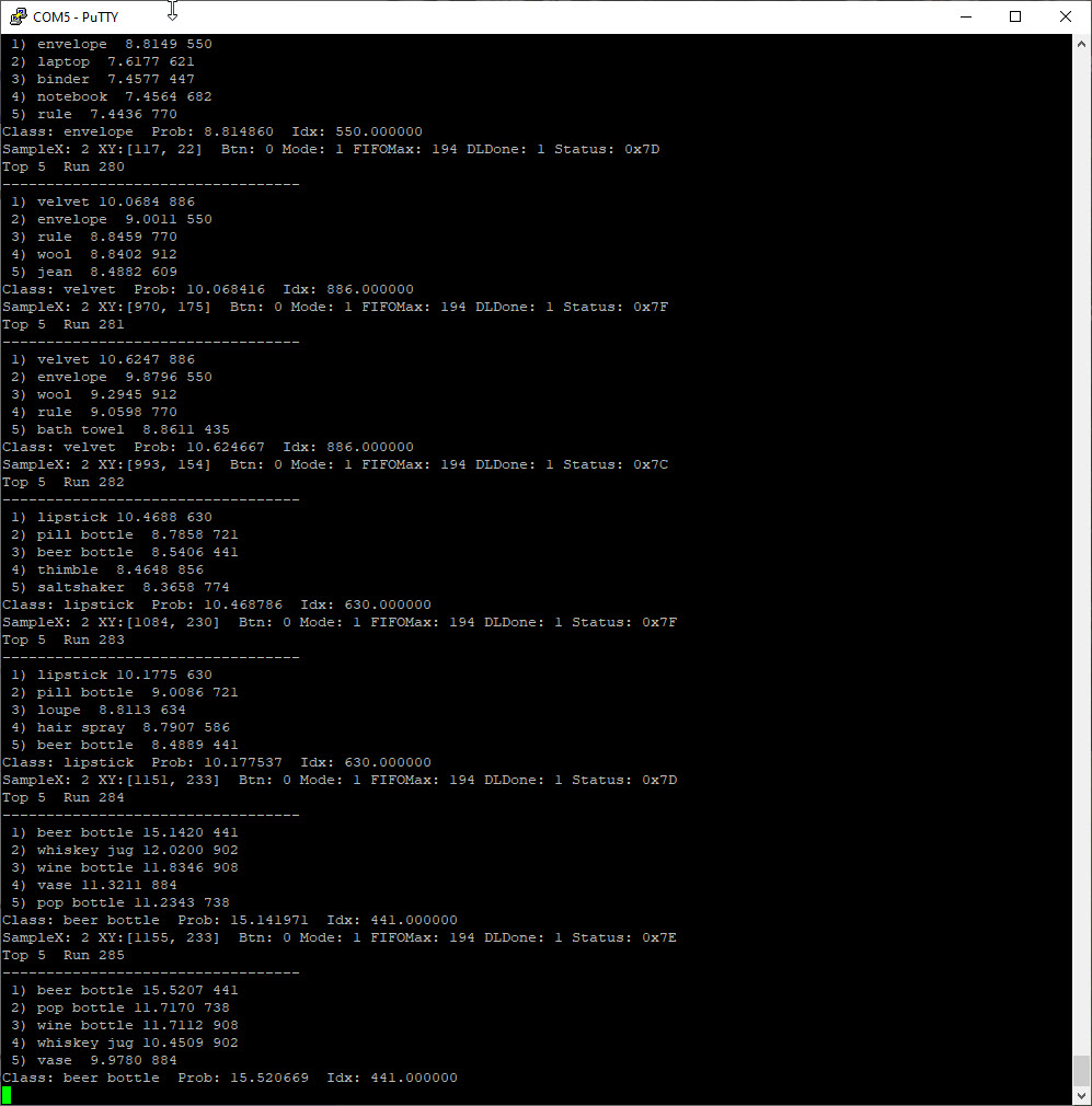
The deep learning processor IP core sends the result back to the external DDR memory. The software model running on the ARM processor retrieves the prediction result and annotates the prediction on the output video stream. This screenshot shows that you can read the ARM processor prediction result by using a serial connection.

This screenshot shows the frame captured from the output video stream which includes the ROI selection and the annotated prediction result.

4. After completing all your verification steps, manually deploy the entire reference design as an executable on the SD card on the ZCU102 board by using the ARM processor. Once the manual deployment is completed a MATLAB connection to the FPGA board is not required to operate the reference design.
See Also
dlhdl.ProcessorConfig | dlhdl.buildProcessor