Hauptinhalt

SPI Controller Transfer

R2026b

Write to and read from SPI device connected to NVIDIA Jetson board

Since R2026a

  • SPI Controller Transfer block

Libraries:
NVIDIA Jetson and NVIDIA DRIVE / Communication

Description

Add-On Required: This feature requires the MATLAB Coder Support Package for NVIDIA Jetson and NVIDIA DRIVE Platforms add-on.

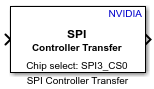
The SPI Controller Transfer block writes data to and reads data from a Serial Peripheral Interface (SPI) device connected to an NVIDIA® Jetson™ boards.

Ports

Input

expand all

Data to write, specified as a scalar or vector.

Data Types: single | double | int8 | int16 | int32 | int64 | uint8 | uint16 | uint32 | uint64

Output

expand all

Data read from the register of the SPI device, returned as a scalar or vector. The output data is the same size and data type as the input data.

Data Types: single | double | int8 | int16 | int32 | int64 | uint8 | uint16 | uint32 | uint64

Parameters

expand all

To edit block parameters interactively, use the Property Inspector. From the Simulink® Toolstrip, on the Simulation tab, in the Prepare gallery, select Property Inspector.

Hardware board to deploy the model to.

Programmatic Use

To set the block parameter value programmatically, use the set_param (Simulink) function.

To get the block parameter value programmatically, use the get_param (Simulink) function.

Parameter: Board
Values: "NVIDIA Jetson TX2 Developer Kit" | "NVIDIA Jetson AGX Xavier Developer Kit" | "NVIDIA Jetson AGX Orin Developer Kit" | "NVIDIA Jetson Xavier NX Developer Kit" | "NVIDIA Jetson Orin Nano Developer Kit" | "NVIDIA Jetson Nano Developer Kit"

Example: set_param(gcb,"Board","NVIDIA Jetson Orin Nano Developer Kit")

Pin connected to the SPI peripheral device. The Board parameter setting determines the available settings, default value, and programmatic parameter name. This table shows the available settings for each board.

Board Parameter SettingAvailable Chip Select Pin SettingsDefault ValueProgrammatic Parameter Name

NVIDIA Jetson AGX Xavier Developer Kit

  • SPI0_CS0

  • SPI0_CS1

SPI0_CS0SSPin1SPI
NVIDIA Jetson TX2 Developer Kit
  • SPI3_CS0

  • SPI3_CS1

SPI3_CS0SSPin1SPIMiscSpidev3
NVIDIA Jetson Orin Nano Developer Kit
  • SPI0_CS0

  • SPI0_CS1

  • SPI1_CS0

  • SPI1_CS1

SPI1_CS0SSPin2SPI
NVIDIA Jetson Nano Developer Kit
  • SPI0_CS0

  • SPI0_CS1

  • SPI1_CS0

  • SPI1_CS1

SPI1_CS0SSPin2SPI
NVIDIA Jetson AGX Orin Developer Kit
  • SPI0_CS0

  • SPI0_CS1

  • SPI2_CS0

  • SPI2_CS1

SPI0_CS0SSPin2SPIMiscSpidev0And2
NVIDIA Jetson Xavier NX Developer Kit
  • SPI0_CS0

  • SPI0_CS1

  • SPI2_CS0

  • SPI2_CS1

SPI0_CS0SSPin2SPIMiscSpidev0And2

Programmatic Use

To set the block parameter value programmatically, use the set_param (Simulink) function.

To get the block parameter value programmatically, use the get_param (Simulink) function.

Parameter: SSPin1SPI
Values: "SPI0_CS0" (default) | "SPI0_CS1"

Example: get_param(gcb,"SSPin1SPI")

Parameter: SSPin1SPIMiscSpidev3
Values: "SPI3_CS0" (default) | "SPI3_CS1"
Parameter: SSPin2SPI
Values: "SPI1_CS0" (default) | "SPI0_CS0" | "SPI0_CS1" | "SPI1_CS1"
Parameter: SSPin2SPIMiscSpidev0And2
Values: "SPI0_CS0" (default) | "SPI0_CS1" | "SPI2_CS0" | "SPI2_CS1"

Mode to use for SPI communication. This table shows the clock polarity and clock phase for each setting.

ModeClock PolarityClock Phase
000
101
210
311

Programmatic Use

To set the block parameter value programmatically, use the set_param (Simulink) function.

To get the block parameter value programmatically, use the get_param (Simulink) function.

Parameter: ClockMode
Values: "0" (default) | "1" | "2" | "3"

Example: set_param(gcb,"ClockMode","2")

Extended Capabilities

expand all

C/C++ Code Generation
Generate C and C++ code using Simulink® Coder™.

GPU Code Generation
Generate CUDA® code for NVIDIA® GPUs using GPU Coder™.

Version History

Introduced in R2026a