Simulation Performance Plots
SoC Blockset™ enables post-simulation analysis of memory diagnostic data. These plots provide high-level performance diagnostics of the memory system of the model. These plots are calculated measurements from a simulation of your model. It considers the data type, sample time, and clock frequency to calculate the bandwidth of your memory model and considers the number of bursts executed per memory port.
To enable signal logging in simulation:
Open the mask of your memory block and select Burst accurate under Memory simulation. The block can be one of the following options:
Open the System on Chip app from the Simulink® toolstrip, and select Profile Memory in the Prepare section.
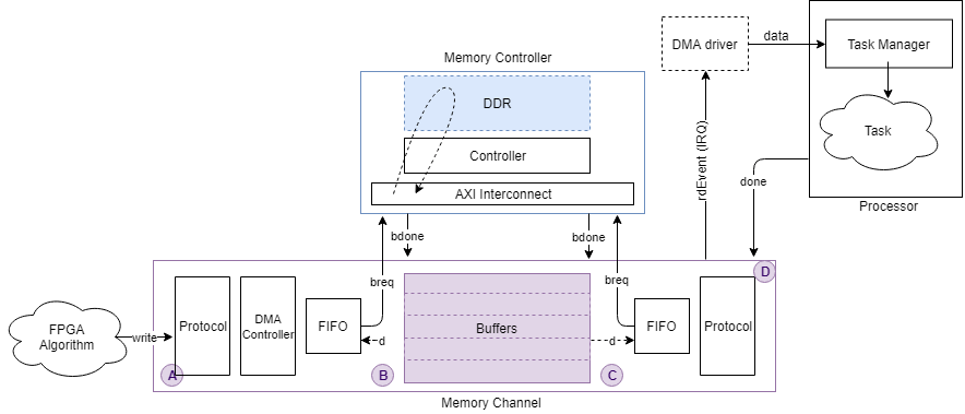
This figure shows the datapath from one FPGA algorithm to another FPGA algorithm through a memory channel.

You can view channel latency plots for the datapath (represented by A, B, C, and D in the following image) on the memory block mask. You can view memory bandwidth, burst count, and control-latency measurements (represented by 1, 2, 3, and 4 in the image) from the Memory Controller block mask.
The datapath from an FPGA algorithm to a processor is served through a DMA driver and a task processor and is illustrated in this image.
Memory Channel Latency Plots
Memory Channel latency information is available post simulation per channel. After simulating your model, open the Memory Channel block mask. On the Performance tab, click Launch performance plots. This action opens a new window with several control options to display these different latencies:
Buffer write complete – This option shows the time it takes between issuing a write request to when the buffer is fully written. It is the path between A and B in the figure.
Buffer read complete – This option shows the time it takes between issuing a read request to when the buffer is read and is available again for writing. It is the path between C and D in the figure. This option is only available if the reader is an FPGA algorithm (not a processor algorithm). If the reader is a processor algorithm, this time shows as zero.
Buffer task execution complete – This option shows the time it takes between issuing a read request to when the buffer is read and is available again for writing. It is the path between C and D in the figure. This option is only available if the reader is a processor algorithm (not an FPGA algorithm). If the reader is an FPGA algorithm, this time shows as zero.
The Buffer task execution complete shows the time it takes for these events to occur:
The write buffer is full.
The channel issued an interrupt request (IRQ) to the processor.
An interrupt service routine (ISR) is executed.
A task is scheduled.
The task started executing.
The task read data.
The task optionally processed the data.
The task sends a
donesignal back to the channel.
This following figure shows the latency path for a task execution to complete, as a red arrow from C to D.

Averaging Window (s) – Specify a time, in seconds, for the averaging window width. The plot is graphed as a moving average, using a time window with the width specified. You can also specify
min,max, orauto.min– Use this value to see data without any averaging. The total latency graph is aligned with the Instantaneous Total Latency marks.max– Use this value to see the overall average for the entire simulation.auto– Use this value to see averaging over the number of buffers in your channel.
Instantaneous Total Latency – This shows discrete total latency measurements per buffer.
If you add Buffer write complete to Buffer read complete or Buffer task execution complete, the plot displays the full latency from writer to reader. This image shows the total latency plot for the Streaming Data from Hardware to Software example.

Note that the latencies are showing over an averaging window of one second. The instantaneous total latency shows a peak in latency as 76.8267 ms. Use this information to verify the model against the requirements.
Memory Controller Latency Plots
Memory controller latency information is available post simulation using the Performance Report app. After simulating your model, follow these steps to view memory controller metrics:
In the Performance Report app, select PS Memory Controller or PL Memory Controller for processing system memory or programmable logic memory, respectively.
Set Select plot type to
Latencies.Set Masters to plot to the master for which you want to view data.
Select the latencies to view. Choose from any of these options:
Burst request to first transfer complete – This option shows the time it takes from the moment the memory block issues a burst-write request to the first transfer of data. This latency accounts for arbitration or interconnect delays. It is the path between 1 and 2 in the figure.
Burst execution latency – This option shows the time it takes from the first transfer of data to when a burst is written to memory. It is the path between 2 and 3 in the figure.
Burst last transfer to complete latency – This option shows the time it takes from the moment a burst completes to when the Memory Controller block issues a
burst-donesignal to the memory block. It is the path between 3 and 4 in the figure.Averaging Window (s) – Specify a time, in seconds, for the averaging window width. The plot is graphed as a moving average, using a time window with the width specified. You can also specify
min,max, orauto.min– Use this value to see data without any averaging. The total latency graph is aligned with the Instantaneous Total Latency marks.max– Use this value to see the overall average for the entire simulation.auto– Use this value to see averaging over 1% of the bursts during the simulation.
Click Create Plot.
This figure shows the datapath from one FPGA algorithm to another FPGA algorithm through a memory channel.
This image shows the total latency for Master
4 in the Analyze Memory Bandwidth Using Traffic Generators example.
The Instantaneous Total Latency shows discrete total latency measurements per burst.

Note
Memory controller latency plots are not available when the master is a processor.
You can then zoom in to analyze the peak instantaneous latency:

Memory Bandwidth Plots
To view memory bandwidth:
In the Performance Report app, set plot type to
Bandwidth.Select the masters for which you want to graph bandwidth.
Click Create Plot.
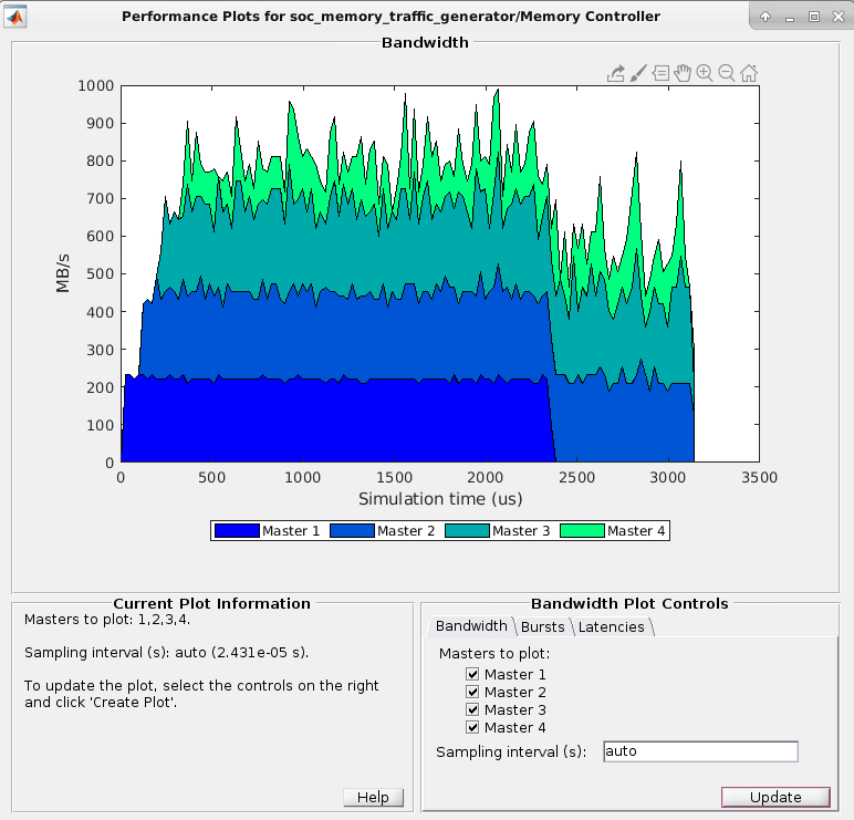
This action plots the bandwidth, in megabytes per second, for the selected masters over the duration of the simulation time. This image shows the bandwidth for the Analyze Memory Bandwidth Using Traffic Generators example.
Note
Bandwidth information is not displayed when a master is a processor.
Memory Burst Plots
In the Performance
Report app, set plot type to Bursts. Then, select
the masters for which you want to graph bursts. Click
Create Plot to see the number of bursts executed for the
selected master over the duration of the simulation time.
This image shows the burst count for the Analyze Memory Bandwidth Using Traffic Generators example.

Note
Bandwidth information is not displayed when a master is a processor.
See Also
AXI4 Random Access Memory | AXI4-Stream to Software | Software to AXI4-Stream | AXI4 Video Frame Buffer | Memory Traffic Generator