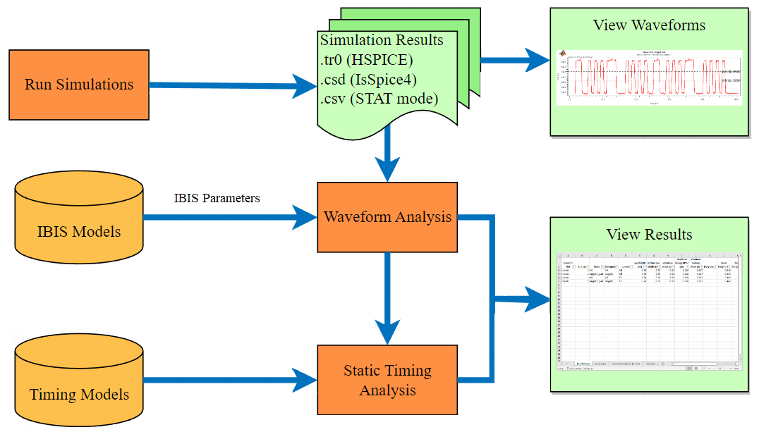
Waveform Analysis
Waveform analysis provides information about waveform overshoot and other quality metrics in parallel link projects. During waveform analysis, the Parallel Link Designer app analyzes every edge of every waveform, applies slew-rate derating, and measures flight times. You need SPICE or STAT mode simulation results to perform waveform analysis.
You can use the Parallel Link Designer app to perform two types of waveform analysis:
Transfer net waveform analysis — The app uses the simulation results of a schematic in pre-layout or an extended net in post-layout.
Standard load waveform analysis —The app uses the simulations created for each driver to measure standard load delay.
Transfer Net Waveform Analysis
Transfer net waveform analysis works directly with the waveform files that the simulator produces. The analysis technique uses algorithms to find edges in the receiver waveforms and correlates the stimulus edges with receiver edges. It also uses 18 threshold voltage levels and multiple check parameters to analyze each edge extensively. The app performs this analysis in five steps:

Find Waveform Edges
The Parallel Link Designer app scans the waveform data at each receiver node and finds an edge to correspond to each stimulus edge. The app skips the first and the last edges. You can also skip additional edges at the start of the waveform. You can specify the number of skipped edges individually for data, strobe, and clock transfer nets in the Simulation Parameters dialog box. To open the dialog box, select Setup > Simulation Parameters....
If the app does not find any edges, it reports errors in the Waveform Fatal tab of the Waveform and Timing Report window.
Measure Edges and Eye
The Parallel Link Designer app measures and checks the edges and the eye diagram. The app checks each edge for overshoot and waveform quality.
The app reports any overshoot violations in the Overshoot Violations tab and all other violations in the Quality Violations tab of the Waveform and Timing Report window. To help you diagnose the error, the app also reports the:
Node where the error occurred,
Time at which the error occurred during simulation
Rule that the edge violated
Value of the violated rule and the amount by which the edge violated it
For more information on how the app defines the waveform and eye processing parameters, see Waveform Processing Parameters and Eye Measurement Parameters.
Measure Raw Etch Delay
The Parallel Link Designer app measures minimum and maximum raw etch delays on the rising and falling edges of the waveform. By default, the app skips the first and the last edges of every waveform. You can specify additional edges to skip in the Simulation Parameters dialog box. To open the dialog box, click Setup > Simulation Parameters... from the app toolstrip.
In the non-STAT Mode, the app measures every edge of every waveform. In the STAT Mode, you can specify the number of edges to measure in the Waveform Analysis Bits parameter in the Simulation Parameters dialog box. You can specify edges to skip in both non-STAT and STAT modes.
The app calculates two types of raw etch delays:
Single-ended — The receiver thresholds used for each delay depend on the target probe point.
Differential — The app measures the delay on the differential waveform (non-inverting minus inverting). The thresholds the app uses are based on the target probe point.
Note
In the STAT mode, the default target probe point is always the pad.
For more information, see Etch Delay Measurement Threshold Parameters.
Perform Slew Rate Derating
You can use the slew rate derating mechanism to adjust the minimum and maximum etch delays by using the measured slew rates at the receiver. This optional step is useful to predict switching times for slew rates other than the nominal value.
The Parallel Link Designer app can automatically perform slew rate derating when the IBIS file contains the derating table. The app measures the slew rates and looks up the derating value in the table for each edge. You can specify the thresholds for slew rate measurement in the IBIS model. The app uses the derated raw etch delay to calculate the etch delay for setup and hold margin calculations in timing analysis.
The Edge Details tab of the Waveform and Timing Report window shows the raw etch delay, derated raw etch delay, and etch delay for each edge. The Derating Details tab of the Waveform and Timing Report window shows the slew rate and derating value applied to each edge.
Calculate Final Etch Delay
The final etch delay calculation subtracts the standard load delay from the derated raw etch delay.
The app uses four etch delay values in the timing analysis for each net: Rmin, Rmax, Fmin, and Fmax. These values are the worst case etch delay values for all the nonskipped edges. The app derives the final etch delay numbers as follows:
Rmin etch delay — Smallest of the Rmin etch delays.
Rmax etch delay — Largest of the Rmax etch delays.
Fmin etch delay — Smallest of the Fmin etch delays.
Fmax etch delay — Largest of the Fmax etch delays.
By using the worst case values over all processed edges, the app accounts for any ISI (Inter-symbol interference) effects in the etch delay values for timing analysis.
Standard Load Waveform Analysis
The standard load simulations include simulations with and without the package. The waveform that the app uses to measure the standard load depends on the source probe point.
| Source Probe Point | Standard Load Waveform |
|---|---|
core | 0.5V on v_stimulus |
SL_pad | stload_sl_wopkg@load |
SL_pin | stload_sl_wpkg@load |
The app performs the analysis in two steps:

Find Waveform Edges
The Parallel Link Designer app scans the waveform data at the load and finds an edge to correspond to each stimulus edge. The app skips the first and the last edges.
If the app does not find any edges, it reports errors in the Fatal Waveform tab of the Waveform and Timing Report window.
Measure Standard Load Delays
The Parallel Link Designer app measures the standard load delays at the second (falling) and third (rising) edges of the load waveform.
For single-ended waveforms, the standard load delay varies from 0.5 V on
v_stimulus to the VmeasR on the rising edge and
VmeasF on the falling edge of the load.
For differential waveforms, the standard load delay varies from 0.5 V on
v_stimulus to 0 V on the differential waveform (noninverting minus
inverting).
Waveform Factors Affecting Interconnect Delay
Some waveform shapes can affect timing. In waveform analysis, the Parallel Link Designer app includes a number of levels and rules that can detect transitions that can cause incorrect interconnect delays, without generating excessive false warnings. Review the generated fatal and quality waveform reports before relying on the timing analysis.
The app defines the setup and hold timing rules assuming a specific slew rate range at
an input. When you use receivers with narrow transition ranges in nets with minimal timing
margins, the slew rates must fall within the vendor specifications. If you use a buffer in
the nets that do not have minimal timing margins, you can widen the
VinMeas ranges instead of constraining the slew rate.
Overshoot violations affect device longevity but do not impact interconnect delays.