Via and Stackup Management in Serial Link Project
The vias are associated with a stackup in the library where they are stored. There can be multiple stackup and via libraries in a project. The first time you edit a via in pre-layout you are prompted for the number of layers to use for the default pre-layout stackup. In post-layout the stackup and vias are from the PCB database by default. Use the Via Editor dialog box by right clicking on the vias in the Pre-Layout Analysis tab to manage them. The elements in the via editor can be divided into three groups: common via elements, pre-layout specific via elements, and post-layout specific via elements.
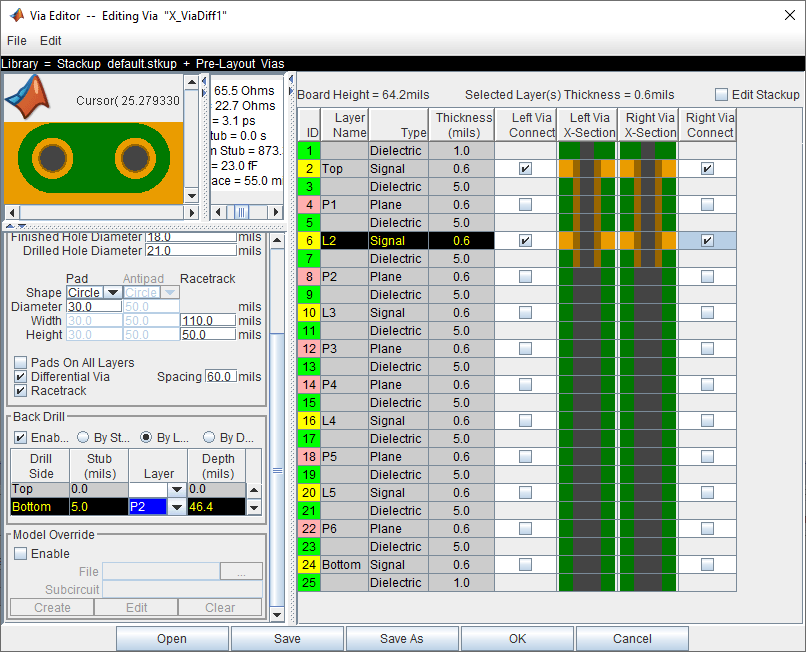
Via Elements
| Via Element | Description |
|---|---|
| Top view and electrical characteristics | The top view shows the via as it would appear when viewed from the top of the board. The electrical characteristics show the impedance, delay backdrill, and other characteristics. The reported delay is for the barrel of the via. |
| Via geometry | You can edit the geometry of the via by defining the start and end layers, hole diameters, and shape and dimensions of the pad and antipad. You can also select if a via model is single-ended or differential. |
| Via backdrill | You can select the depth of via backdrill by stub, layer, or depth. |
| Override via model | You can override a via model by using your custom subcircuit saved in one of the SPICE libraries. |
| Connect via layers | The Left Via Connect column is used to select the layer connections that will appear on the left side of the via symbol. The Right Via Connect column is used to select the layer connections that will appear on the right side of the via symbol. A layer is connected when the checkbox for that layer is checked. The Via X-Section columns show a representation of the via cross section. |
| Modify stackup | To modify the stackup, check the Edit Stackup checkbox. |
There are several important definitions for vias and pins:
A via under a BGA is a via, not a pin.
A through hole connector padstack is a pin, not a via.
A connector means a multi-board mated connector (connects two board Instances).
Editing Via for Pre-Layout Simulations
To edit vias for pre-layout simulation, open the Via Editor dialog box by selecting Tools > Via Editor or by right-clicking on a via schematic symbol and selecting Edit Differential Via Model or Edit Single Ended Via Model. You need to enter the number of conducting layers for the default stackup the first time you open the Via Editor dialog box.
The Via Editor works in a selected library. Vias can be edited, added or deleted from a library. In pre-layout, the Via Editor creates a default library that contains a default via model and a default stackup. The Library operations can be selected from the File menu.
Editing Via for Post-Layout Simulations
The Padstack/Trace Manager is used to view and manage overrides to padstacks and traces in post-layout as well as manage backdrilling of pins and vias by net, RefDes or Part. You can edit the geometry of a single via, or multiple vias at one time. You can also assign overrides by individual instance of a padstack or by occurrence of each padstack’s library name in the database.
Back Drill Setup Tab
The Back Drill Setup tab allows backdrill information to be viewed and changed by net, by padstack, by RefDes, or by Part by selecting from the View Mode list. In each case the backdrill can be turned on or off. The view modes are:
Back Drill by Net — One row per Extended Net per Board.
Back Drill by Padstack — One row per Padstack.
Back Drill by RefDes — One row per Reference Designator.
Back Drill by Part — One row per Part Number.
The Back Drill Setup tab is only enabled if backdrilling is enabled on one or more boards on the Stackup tab of the Setup Board dialog.
Via/Pin Editor Tab
Padstack models are created automatically from the PCB data for vias, surface mount pads and through-hole pins using the internal padstack solver.
Padstack Definitions
| Padstack Elements | Definitions |
|---|---|
| Padstack | The geometry information from the PCB database. Contains the start and end layer of the padstack, barrel dimensions, etc. A Padstack does not contain the layers connected or XY coordinates. |
| Padstack Configuration | A Padstack plus layer connections. A Padstack Configuration does not contain XY coordinates. |
| Padstack Configuration Instance | A Padstack Configuration at a specific XY coordinate on a board. A specific via has geometry, connectivity and a location on a PCB. A specific pin has geometry, connectivity, a location, a reference designator and a pin number |
A Padstack can be used for multiple Padstack Configurations. A Padstack Configuration can be used for multiple Padstack Configuration Instances.
Padstack Editor View Modes
The views are selected from the list on the Via/Pin tab. The view modes correspond to the definitions above. In each view mode there is one row for each item of the selected type:
Padstack (Geometry) — One row per Padstack. This rolls up all Padstack Configurations and Padstack Configuration Instances that use a Padstack.
Padstack Configuration (Connectivity) — One row per Padstack Configuration. This rolls up all Padstack Configuration Instances that use a Padstack Configuration.
Padstack Configuration Instance — One row per Padstack Configuration Instances.
Padstack Editor Edit Modes
The padstack editor has two modes:
Padstack — All changes made in the editable columns apply to the padstack. This means all Padstack Configuration Instances that use the same Padstack as the row being edited will change. For example, if the View Mode is Padstack Configuration Instance and the Edit Mode is Padstack, a change to one row is applied to all rows that have the same Padstack.
Instance — All changes apply to the Padstack Configuration Instance only. For example, if the View Mode is Padstack Configuration Instance and the Edit Mode is Instance, a change to one row is only applied to that row.
Common Operations
| Editing geometry of a single via | To edit the geometry of a single via (one via at one XY coordinate), use the Padstack Configuration Instance View Mode and the Instance Edit Mode. Any changes to the geometry is applied to the specific via edited when in this mode. |
| Editing using the Via Editor | Right-click on a row and choose Visual Via Editor from the menu. |
| Changing the Padstack | To change the Padstack that a Padstack Configuration Instance is based on, use the Padstack Configuration Instance View Mode and in the Base Padstack column choose a different Padstack. The list of padstacks are the padstacks that share the same start and end layer with the original padstack for this Padstack Configuration Instance. |
| Editing a Padstack | To edit a Padstack, use the View Mode Padstack. The behavior depends on Edit Mode:
|
| Overriding a via model | Via models are typically done with connectivity to specific layers. Therefore, the Padstack Configuration View Mode or the Padstack Configuration Instance View Mode are used to override a via model. In both modes the Model Override column is part of the table. To override a model right-click and select one of:
If the View Mode is Padstack Configuration the model is applied to every Padstack Configuration Instance that uses that Padstack Configuration. If the View Mode is Padstack Configuration Instance the model is applied to the single Padstack Configuration Instance that you edited. Note The edit mode must be Padstack. |
Trace Overrides Tab
The Trace Overrides tab of the Padstack/Trace Manager is used for trace model overrides. The lossy transmission line models for traces created by the field solver from the stackup and trace width can be overridden with user-provided models. The Trace Overrides tab shows the trace widths on each layer of each board.
The models used for overrides are assumed to be RLGC models with one model per file, and the base name of the file must be the same as the model name.
For single-ended traces there is one row for each trace width found on each layer. Select one or more rows and click the Select Model button to browse to a transmission line model in the library.
For differential traces, there is one row for each trace width on each layer, and columns for differential separation and coupling layer. The coupling layer is a list containing the same layer and any adjacent signal or mixed layers. Select an adjacent layer for broadside coupled differential traces. When a separation is added a new row is created for that layer and trace width. This allows models for multiple separations to be specified for each width on each layer.
The tolerance for overrides is 0.1 mm in width. In other words, if an override is specified for a trace of width 4.0 mm on a layer, the override is applied to all traces with widths from 3.9 mm to 4.1 mm on that layer.
Example One-Conductor Model
For file name
sl_55ohm.mod:
model sl_55ohm W ModelType=RLGC N=1
+ Lo = +3.60600E-07
+ Co = +1.20300E-10
+ Ro = +6.07368E+00
+ Rs = +1.48880E-03
+ Gd = +1.89000E-11
Example Differential Model
For file name
sl_55ohm_diff.mod:
.model sl_55ohm_diff W ModelType=RLGC N=2
+ Lo = +3.58800E-07 +4.84700E-08 +3.58800E-07
+ Co = +1.23200E-10 -1.66400E-11 +1.23200E-10
+ Ro = +6.07368E+00 +0.00000E+00 +6.07368E+00
+ Rs = +1.50556E-03 +1.12767E-04 +1.50556E-03
+ Gd = +1.93500E-11 -2.61400E-12 +1.93500E-11