cadnet
R2026bDescription
Create a cadnet object
A cadnet is a designated grouping of interconnected pcb components in a PCB layout.
Creation
Description
cadobj = cadnet(
creates a cadnet object from a pfile,'CadnetName')pcbFileRead object and given a specified
name.
Input Arguments
Properties
Object Functions
show | Show |
cadnetData | Cadnet data |
shapes | Shapes |
Examples
This example shows how to read an Allegro file and create a pcbFileRead object. After this the following operations will be executed:
Create layer, cadnet, padstack, part, and component objects form the
pcbFileReadobjectCreate a powerDistributionNetwork object from the cadnet object
Set the properties of the powerDistributionNetwork object for voltage and current density analysis
Analyze and visualize the voltage and current density
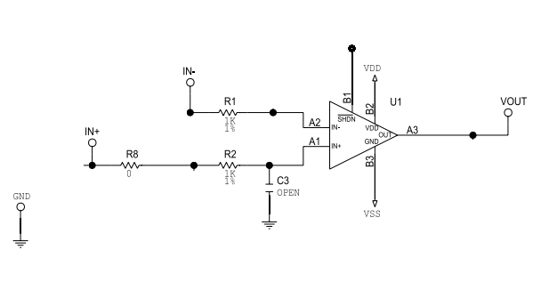
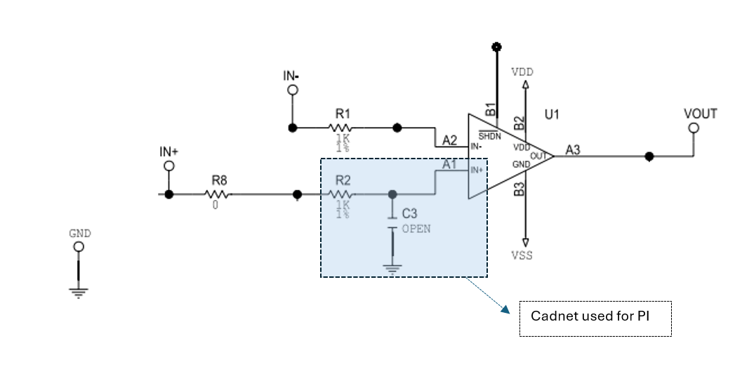
Here is the circuit:
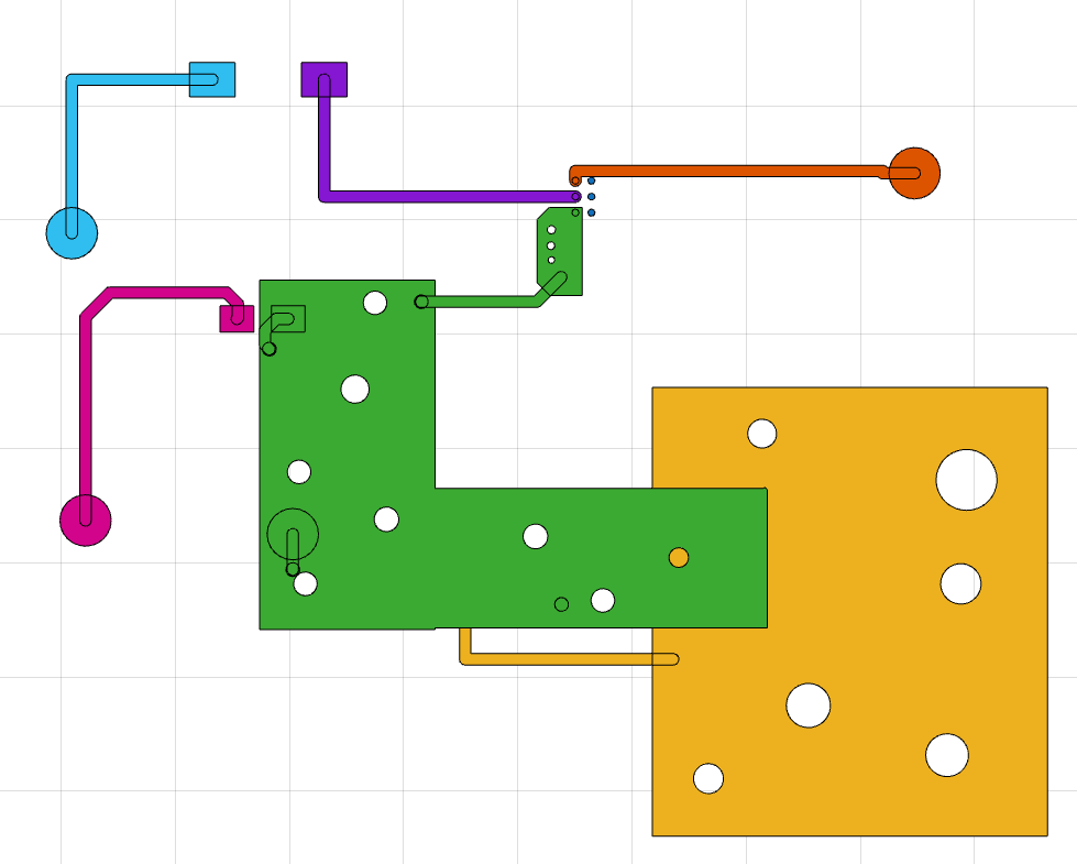
Here is the pcb layout:
Read file
Read a native format Allegro file and look at the properties of the pcb.
pfile = pcbFileRead('native_ExampleBoard_Allegro')pfile =
pcbFileRead with properties:
FileName: 'native_ExampleBoard_Allegro'
NumLayers: 5
MetalLayer: [1 3 5]
DielectricLayer: [2 4]
LayerHeight: [0.0184 0.0104 0.0092 0.0012 0]
NumCadnets: 7
NumPadStacks: 6
NumComponents: 8
NumParts: 5
cadnetList(pfile)
ans = 7×4 table
    CadnetIdx        CadnetName         NumPins    Length
    _________    ___________________    _______    ______

        1        {'Unconnected_Net'}       3           0
        2        {'NET_OUTV'       }       2       0.615
        3        {'NET_GND'        }       1        0.46
        4        {'NET_IN22'       }       2       0.645
        5        {'NET_IN11'       }       4       0.488
        6        {'NET_INNEG'      }       2       0.515
        7        {'NET_INPOS'      }       2       0.676

	Get insights using Copilot
componentList(pfile)
ans = 8×3 table
    ComponentIdx    ComponentName    NumPins
    ____________    _____________    _______

         1            {'OUT_V'}         1
         2            {'U1'   }         6
         3            {'C3'   }         2
         4            {'R1'   }         2
         5            {'TP1'  }         1
         6            {'R2'   }         2
         7            {'IN_N' }         1
         8            {'IN_P' }         1

	Get insights using Copilot
partList(pfile)
ans = 5×2 table
    PartIdx       PartName
    _______    _______________

       1       {'IOSINGLEPIN'}
       2       {'IC6ANT'     }
       3       {'CAPGEN080'  }
       4       {'RESGENH40'  }
       5       {'RESGEN080'  }

	Get insights using Copilot
padStackList(pfile)
ans = 6×2 table
    PadstackIdx        PadstackName
    ___________    ____________________

         1         {'MHYCIRCLE009'    }
         2         {'MHYC012'         }
         3         {'MHYRECT46X59'    }
         4         {'MHYRECT80X60H40' }
         5         {'VIA'             }
         6         {'MHYRECT46X59_TOP'}

	Get insights using Copilot
stackUp(pfile)
ans = 5×8 table
    LayerNumber      LayerName         LayerType        Material     Thickness(inch)    EpsilonR    LossTangent    Conductivity(S/m)
    ___________    ______________    ______________    __________    _______________    ________    ___________    _________________

         1         {'TOP'       }    {'Signal'    }    {'COPPER'}        0.0012             1              0           5.96e+07
         2         {'Dielectric'}    {'Dielectric'}    {'FR-4'  }         0.008           4.5          0.035                  0
         3         {'LAYER2'    }    {'Plane'     }    {'COPPER'}        0.0012             1              0           5.96e+07
         4         {'Dielectric'}    {'Dielectric'}    {'FR-4'  }         0.008           4.5          0.035                  0
         5         {'BOTTOM'    }    {'Signal'    }    {'COPPER'}        0.0012             1              0           5.96e+07

	Get insights using Copilot
Create layer object
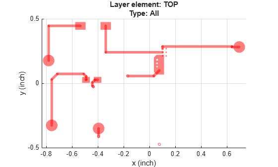
Create and visualize a layer object.
layerobj = layer(pfile,1,Type= 'All')layerobj =
layer with properties:
pcBoard: [1×1 pcbFileRead]
LayerNumber: 1
Type: "All"
LayerHeight: 0.0184
NumSurfaces: 1
NumPins: 14
NumVias: 4
NumTraces: 21
EntityList: [1×1 struct]
show(layerobj)
Create a cadnet object
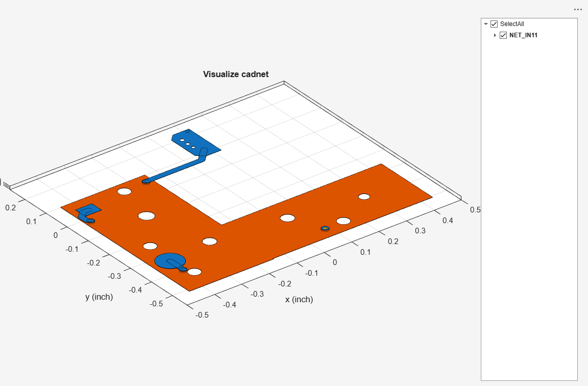
Create cadnet object and look at its data.
cadobj = cadnet(pfile,'NET_IN11')cadobj =
cadnet with properties:
pcBoard: [1×1 pcbFileRead]
CadnetName: 'NET_IN11'
NumPins: 4
NumSurfaces: 2
NumVias: 4
NumTraces: 4
TotalLength: 0.4880
Voltage: 'NoDef'
LayerRange: [1 3 5]
EntityList: [1×1 struct]
figure
show(cadobj)
Create a padstack object
Create a padstack object and look at its data.
stackobj = padStack(pfile,'MHYC012')stackobj =
padStack with properties:
pcBoard: [1×1 pcbFileRead]
PadStackName: 'MHYC012'
Stack Definition:
StartLayer: 'TOP'
StopLayer: 'TOP'
LayerStack: "TOP"
Pad, Antipad and Drill Geometry:
LayerwiseGeometry: [1×4 table]
Padstack Occurrence
NumPadStack: 6
PadType: 'Pin'
PadCenter: [6×2 double]
PinPadInfo: [6×8 table]
shapes(stackobj)
ans =

  dictionary (string ⟼ antenna.Polygon) with 1 entry:

    "TOP" ⟼ 1×1 antenna.Polygon
Create a part object
Create a part object and look at its data.
partobj = part(pfile,"IC6ANT")partobj =
part with properties:
pcBoard: [1×1 pcbFileRead]
PartName: 'IC6ANT'
NumComponents: 1
ComponentInfo: [1×7 table]
componentData(partobj)
ans =
  component with properties:

             pcBoard: [1×1 pcbFileRead]
       ComponentName: 'U1'
            PartName: 'IC6ANT'
       ComponentType: 'IC'
             NumPins: 6
               Value: ''
            Facement: 'TOP'
    ComponentPinInfo: [6×7 table]
Create component object
Create a component object and look at its pin data.
componentobj = component(pfile,'U1')componentobj =
component with properties:
pcBoard: [1×1 pcbFileRead]
ComponentName: 'U1'
PartName: 'IC6ANT'
ComponentType: 'IC'
NumPins: 6
Value: ''
Facement: 'TOP'
ComponentPinInfo: [6×7 table]
componentPinData(componentobj,1)
ans =
  pinsData with properties:

             PinShape: 'Circle'
           PartNumber: 'IC6ANT'
            Component: 'U1'
            PinNumber: 'A3'
                Value: ''
             PadStack: 'MHYC012'
           CadnetName: 'NET_OUTV'
           StartLayer: 1
            StopLayer: 1

   Circular pin dimensions:
               Center: [0.1010 0.2690]
             Diameter: 0.0120
    DrillHoleDiameter: 0
Create a power distribution network object
Create a power distribution network object from a cadnet object. After this the following operations can be performed:
Set up the Network Parameters, DC Parameters, and DC Rules properties of the power distribution network for power integrity analysis
Analyze and visualize the voltage and current density of the power distribution network
Here is the cadnet for power integrity analysis.
pdnobj = powerDistributionNetwork(cadobj)
pdnobj =
  powerDistributionNetwork with properties:

   Network Parameters:
              NetType: [1×1 cadnet]
               Source: {}
                 Load: {}
                Sense: {}
     PlatingThickness: []

   DC Parameters:
       NominalVoltage: []
          LoadCurrent: []

   DC Rules
    MaxCurrentDensity: []
           MinVoltage: []
           MaxVoltage: []
        MaxViaCurrent: []

To Analyse PDN:
Set Network Parameters: setNetworkParameters
Set DC Parameters: setDCParameters
Set DC Rules: setDCRules
Find the pins connected to the cadnet using the findComponents function.
ConnPins = findComponents(cadobj)
ConnPins = 4×5 table
    ComponentIndex    Refdes    PinList    ComponentType          Part
    ______________    ______    _______    ______________    _______________

          1           "C3"       "1"       {'Capacitor' }    {'CAPGEN080'  }
          2           "R2"       "2"       {'Resistor'  }    {'RESGEN080'  }
          3           "TP1"      "1"       {'Test Point'}    {'IOSINGLEPIN'}
          4           "U1"       "A1"      {'IC'        }    {'IC6ANT'     }

	Get insights using Copilot
in = ConnPins.Refdes(2);
out = [ConnPins.Refdes(1),ConnPins.Refdes(4)];
SensePin = ConnPins.Refdes(3);
Set the network parameters.
setNetworkParameters(pdnobj,Source=in,Load=out,Sense=SensePin,PlatingThickness=0.0003);
  powerDistributionNetwork with properties:

   Network Parameters:
              NetType: [1×1 cadnet]
               Source: "R2"
                 Load: ["C3"    "U1"]
                Sense: "TP1"
     PlatingThickness: 3.0000e-04

   DC Parameters:
       NominalVoltage: []
          LoadCurrent: []

   DC Rules
    MaxCurrentDensity: []
           MinVoltage: []
           MaxVoltage: []
        MaxViaCurrent: []

To Analyse PDN:
Set DC Parameters: setDCParameters
Set DC Rules: setDCRules
Set the DC parameters.
setDCParameters(pdnobj,"LoadCurrent",[10e-3,10e-3],"NominalVoltage",2)
  powerDistributionNetwork with properties:

   Network Parameters:
              NetType: [1×1 cadnet]
               Source: "R2"
                 Load: ["C3"    "U1"]
                Sense: "TP1"
     PlatingThickness: 3.0000e-04

   DC Parameters:
       NominalVoltage: 2
          LoadCurrent: [0.0100 0.0100]

   DC Rules
    MaxCurrentDensity: []
           MinVoltage: []
           MaxVoltage: []
        MaxViaCurrent: []

To Analyse PDN:
Set DC Rules: setDCRules
Set the DC rules.
setDCRules(pdnobj,MinVoltage=1,MaxVoltage=2.00002,MaxCurrentDensity=4,MaxViaCurrent=2.0)
  powerDistributionNetwork with properties:

   Network Parameters:
              NetType: [1×1 cadnet]
               Source: "R2"
                 Load: ["C3"    "U1"]
                Sense: "TP1"
     PlatingThickness: 3.0000e-04

   DC Parameters:
       NominalVoltage: 2
          LoadCurrent: [0.0100 0.0100]

   DC Rules
    MaxCurrentDensity: 4
           MinVoltage: 1
           MaxVoltage: 2.0000
        MaxViaCurrent: 2
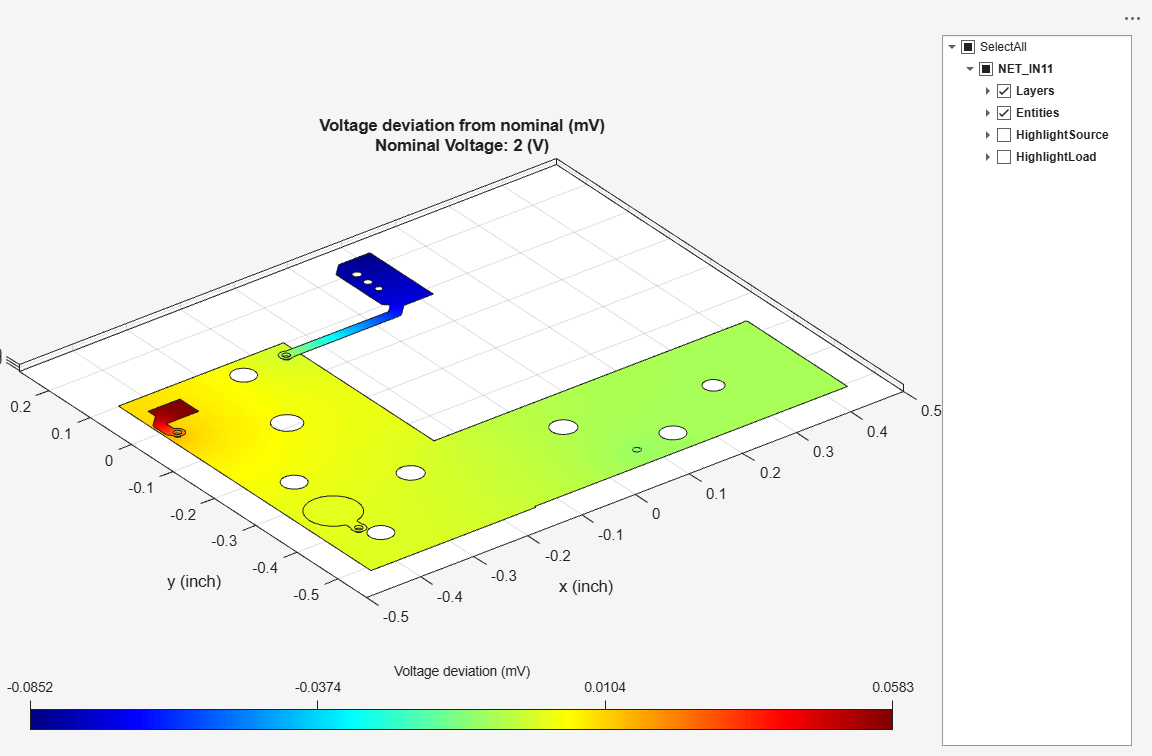
Analyze voltage deviation.
voltage(pdnobj);
Analyze current density with direction enabled.
current(pdnobj,Direction="on")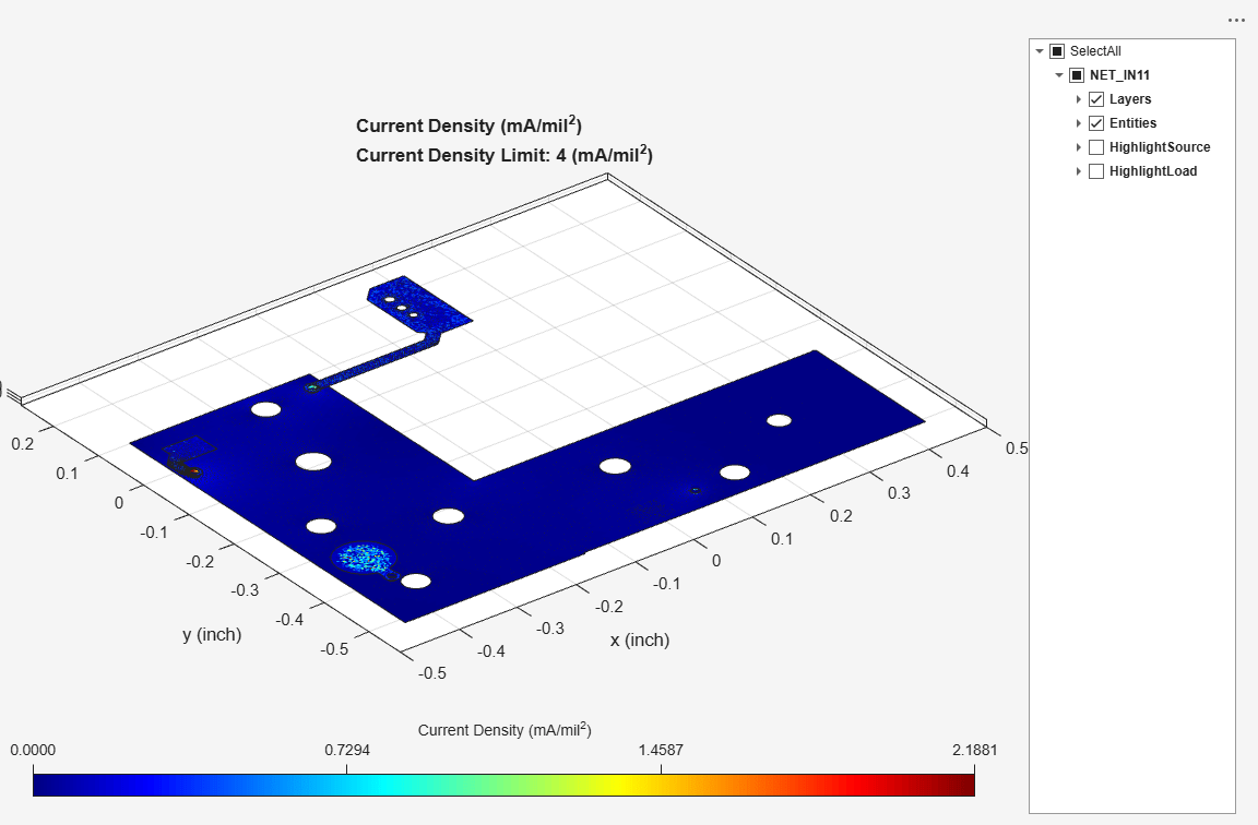
Version History
Introduced in R2025aSee Also
findComponents | powerDistributionNetwork | pcbFileRead | cadnetList

