Modeling Best Practices for FPGA HIL Deployment
For hardware-in-the-loop (HIL) simulation of your Simscape™ plant model, you first configure your model to generate HDL code and simulate it. Hardware deployment of such models has certain requirements that you need to address early in the design process. Understanding how your design maps to your target device is key to generating HDL code that meets your needs when implemented downstream.
CPU and FPGA Data Exchange
Before you deploy your model onto hardware, your model must meet timing constraints required for CPU and FPGA synchronization. The CPU and FPGA operate at different clock cycles (sample rate) which are not synchronized by default. The CPU can achieve model time steps in microseconds, while the FPGA can achieve time steps in nanoseconds. A communication bus enables data transfer between the CPU and FPGA. The figure shows the CPU time step and the FPGA clock cycle for CPU-FPGA data transfer through a communication bus.
When you deploy a real-time model onto a CPU, a timer triggers the CPU at regular intervals (CPU Time Step) to execute CPU instructions sequentially.
For FPGA deployment, you can convert your Simscape plant model to HDL code and synthesize into a bitstream. The bitstream sets up the FPGA resources to replicate your model functionality.
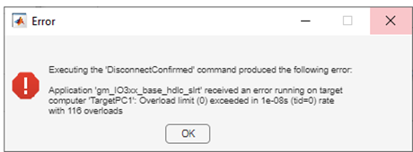
Sometimes a real-time application running on the target computer (CPU of real-time target machine, for example, Speedgoat® real-time target machine) does not have enough time to complete processing before the next time step. This means that the data sent by the faster-running FPGA is beyond the feasible range that CPU can handle. This condition is called a CPU overload. An overload is registered every time an execution step is triggered while the previous step is running. When deploying your model to hardware, you might encounter this error if there is a CPU overload:
For example, consider the sschdlexResonantLLCConverterExample model.
The components inside the FPGA Subsystem block run on an FPGA board and the components that
are outside the FPGA Subsystem block run on a CPU in real time. To learn more, see Resonant LLC Converter for Real-Time FPGA Deployment.
Handling CPU Overloads During CPU-FPGA Data Transfers
The sample time at which the FPGA Subsystem block runs is 20 nanoseconds
(FPGA sample rate ts_fpga), and the other components outside this
subsystem run at a lower sample time (CPU sample rate ts_cpu). The
difference in sample time can cause a CPU overload because the data received at CPU from the
faster-running FPGA might be beyond the feasible range that CPU can handle. This can result
in an error during deployment of the model onto the hardware.
To avoid CPU overload during execution, ensure that all the sample rates in the generated Simulink® Real-Time™ (SLRT) interface model are within the range that the CPUs can process. For hardware deployment, exclude any FPGA-related faster sample rates from the SLRT interface model. To achieve this in the Simscape model:
Insert Rate Transition blocks at the input and output ports of the Simscape subsystem that you want to map to the PCIe interface.
Set the Output port sample time block parameter to
-1.Add a Signal Specification block in the Simscape subsystem and set the Sample time block parameter to the FPGA rate.
These settings can reduce CPU overloads encountered during hardware deployment of your plant model.
Then, you generate your Simulink Real-Time (SLRT) interface model, which must operate at a sample rate that is feasible to the CPU. All the inputs to the Simscape subsystem (FPGA Subsystem in this model) in your SLRT interface model must inherit the same CPU rates. Therefore, if you insert any Rate Transition block, you can avoid manual intervention before deployment by using these settings and ensure that all the sample rates in the generated SLRT interface model are within CPU feasible range.
See Also
sschdladvisor | hdladvisor | Rate Transition | HDL Workflow Advisor Tasks | Getting Started with the HDL Workflow Advisor
Topics
- Basic Principles of Modeling Physical Networks (Simscape)
- Essential Physical Modeling Techniques (Simscape)
- Deploy Simscape DC Motor Model to Speedgoat FPGA IO Module
- Resonant LLC Converter for Real-Time FPGA Deployment